Click to expand full text
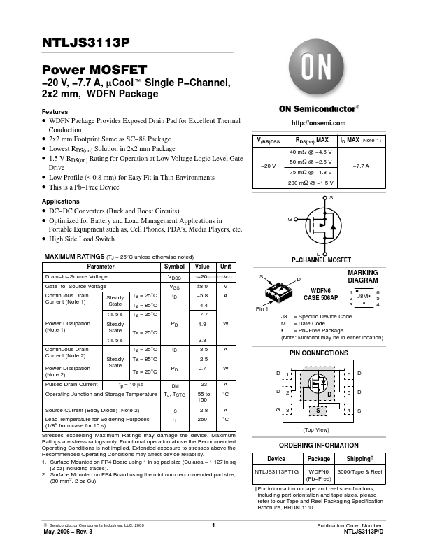
NTLJS3113P Power MOSFET
Features
−20 V, −7.7 A, mCoolt Single P−Channel, 2x2 mm, WDFN Package
• WDFN Package Provides Exposed Drain Pad for Excellent Thermal • • • • •
Conduction 2x2 mm Footprint Same as SC−88 Package Lowest RDS(on) Solution in 2x2 mm Package 1.5 V RDS(on) Rating for Operation at Low Voltage Logic Level Gate Drive Low Profile (< 0.8 mm) for Easy Fit in Thin Environments This is a Pb−Free Device
V(BR)DSS
http://onsemi.com
RDS(on) MAX 40 mW @ −4.5 V −20 V 50 mW @ −2.5 V 75 mW @ −1.8 V 200 mW @ −1.5 V S −7.7 A ID MAX (Note 1)
Applications
• DC−DC Converters (Buck and Boost Circuits) • Optimized for Battery and Load Management Applications in •
Portable Equipment such as, Cell Phones, PDA’s, Media Players, etc.
 NTLJS3113P Datasheet