Full PDF Text Transcription for NTD110N02R (Reference)
Note: Below is a high-fidelity text extraction (approx. 800 characters) for
NTD110N02R. For precise diagrams, and layout, please refer to the original PDF.
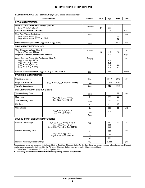
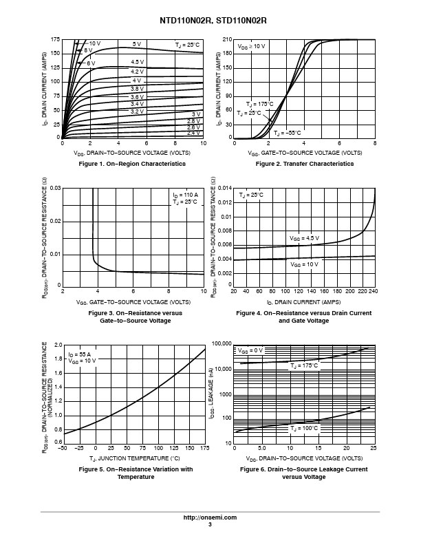
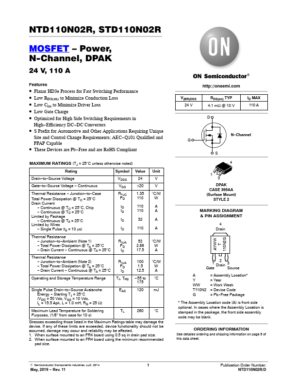
NTD110N02R, STD110N02R MOSFET – Power, N-Channel, DPAK 24 V, 110 A Features • Planar HD3e Process for Fast Switching Performance • Low RDS(on) to Minimize Conduction Loss...
View more extracted text
r Fast Switching Performance • Low RDS(on) to Minimize Conduction Loss • Low Ciss to Minimize Driver Loss • Low Gate Charge • Optimized for High Side Switching Requirements in High−Efficiency DC−DC Converters • S Prefix for Automotive and Other Applications Requiring Unique Site and Control Change Requirements; AEC−Q101 Qualified and PPAP Capable • These Devices are Pb−Free and are RoHS Compliant MAXIMUM RATINGS (TJ = 25°C unless otherwise noted) Rating Symbol Value Unit Drain−to−Source Voltage Gate−to−Source Voltage − Continuous Thermal Resistance − Junction−to−Case Total Power Dissipation @ TC = 25°C Drain Current − Cont
 NTD110N02R Datasheet