http://onsemi. com
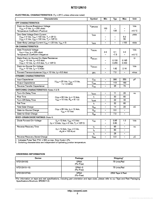
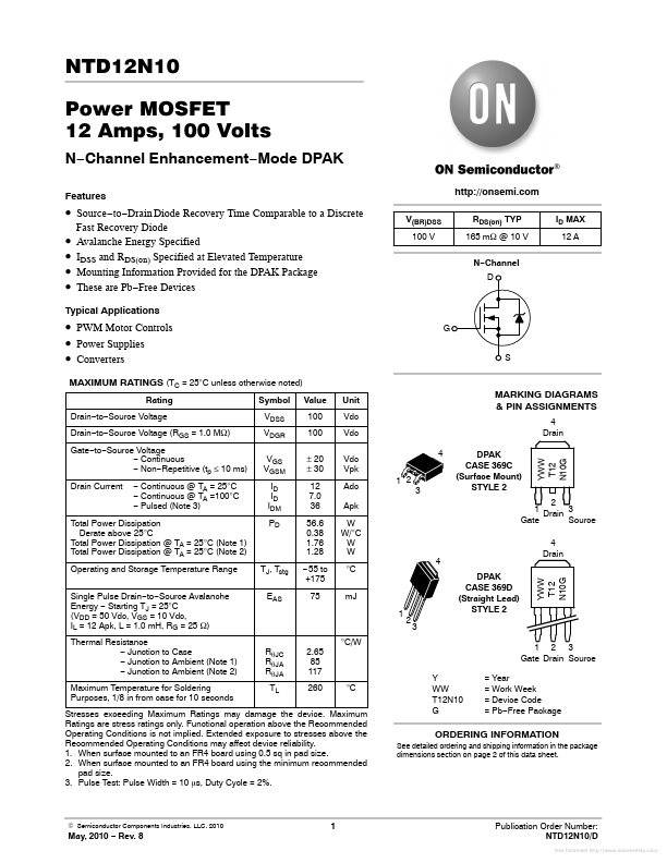
V(BR)DSS 100 V RDS(on) TYP 165 mW @ 10 V N.
Channel D ID MAX 12 A.
Source.
to.
Drain Diode Recovery Time Comparable to a Discrete.
Fast Recovery Diode Avalanche Energy Specified IDSS and RDS(on) Specified at Elevated Temperature Mounting Information Provided for the DPAK Package These are Pb.
Full PDF Text Transcription for NTD12N10 (Reference)
Note: Below is a high-fidelity text extraction (approx. 800 characters) for
NTD12N10. For precise diagrams, and layout, please refer to the original PDF.
NTD12N10 Power MOSFET 12 Amps, 100 Volts N−Channel Enhancement−Mode DPAK Features http://onsemi.com V(BR)DSS 100 V RDS(on) TYP 165 mW @ 10 V N−Channel D ID MAX 12 A • Sou...
View more extracted text
V(BR)DSS 100 V RDS(on) TYP 165 mW @ 10 V N−Channel D ID MAX 12 A • Source−to−Drain Diode Recovery Time Comparable to a Discrete • • • • Fast Recovery Diode Avalanche Energy Specified IDSS and RDS(on) Specified at Elevated Temperature Mounting Information Provided for the DPAK Package These are Pb−Free Devices Typical Applications • PWM Motor Controls • Power Supplies • Converters MAXIMUM RATINGS (TC = 25°C unless otherwise noted) Rating Drain−to−Source Voltage Drain−to−Source Voltage (RGS = 1.
 NTD12N10 Datasheet