Datasheet4U Logo Datasheet4U.com

NB3V60113GV3 - 1.8 V 12.288 MHz OmniClock Generator

Features

  • Member of the OmniClock Family of Programmable Clock Generators.
  • Operating Power Supply: 1.8 V ± 0.1 V.
  • I/O Standards.
  • Input: 6.144 MHz Reference Clock (LVCMOS).
  • Output: 12.288 MHz (LVCMOS).
  • Output Drive Current for Single Ended Output: 8 mA.
  • Power Saving Mode through Power Down Pin.
  • Temperature Range.
  • 40°C to 85°C.
  • Packaged in 8.
  • Pin WDFN.
  • These are Pb.
  • Free Devices Typical Applicati.

📥 Download Datasheet

Datasheet preview – NB3V60113GV3

Datasheet Details

Part number NB3V60113GV3
Manufacturer Onsemi
File Size 84.63 KB
Description 1.8 V 12.288 MHz OmniClock Generator
Datasheet download datasheet NB3V60113GV3 Datasheet
Additional preview pages of the NB3V60113GV3 datasheet.
Other Datasheets by ON Semiconductor

Full PDF Text Transcription

Click to expand full text
NB3V60113GV3 1.8 V 12.288 MHz OmniClock Generator with Single Ended (LVCMOS) Output 
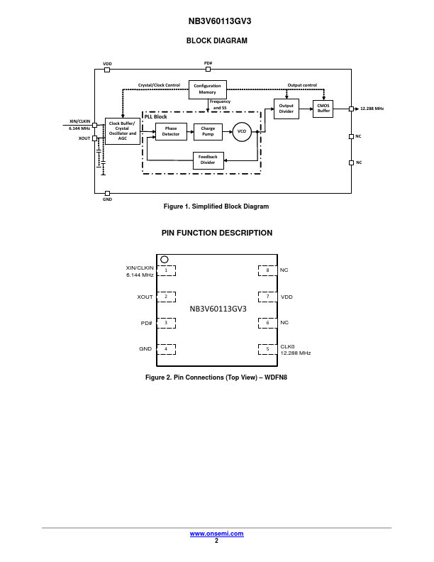
The NB3V60113GV3, which is a member of the OmniClock family, is a low power PLL−based clock generator. The device accepts a 6.144 MHz single ended (LVCMOS) reference clock as input. It generates one single ended (LVCMOS) output of 12.288 MHz. The device can be powered down using the Power Down pin (PD#). Features • Member of the OmniClock Family of Programmable Clock Generators • Operating Power Supply: 1.8 V ± 0.1 V • I/O Standards ♦ Input: 6.144 MHz Reference Clock (LVCMOS) ♦ Output: 12.
Published: |