Datasheet Details
| Part number | NB3V60113G |
|---|---|
| Manufacturer | Onsemi |
| File Size | 264.84 KB |
| Description | 1.8V Programmable OmniClock Generator |
| Datasheet |
 NB3V60113G Datasheet NB3V60113G Datasheet
|
|
|
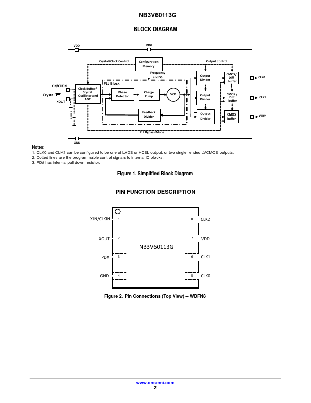
Figure 2.
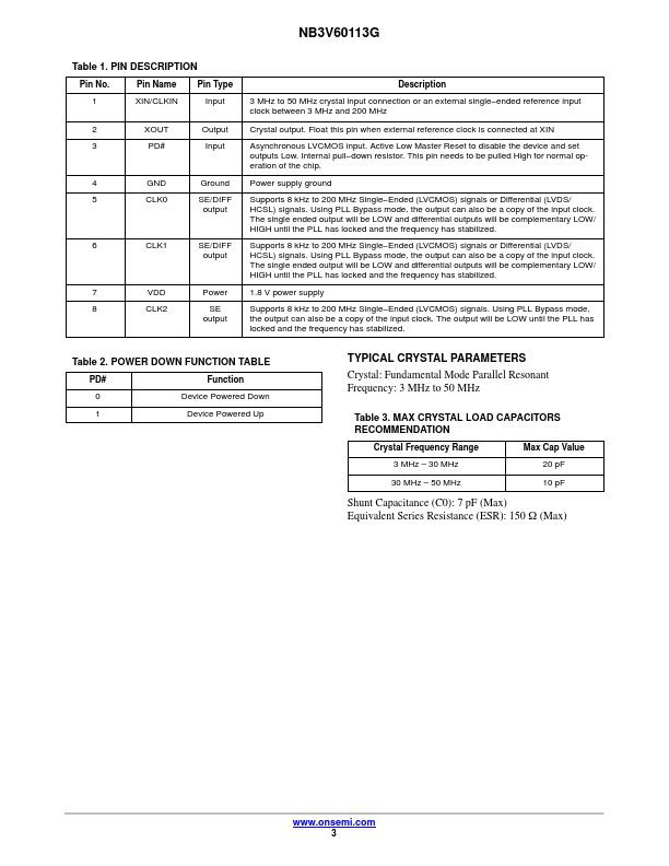
Table 1.
Pin No.
| Part number | NB3V60113G |
|---|---|
| Manufacturer | Onsemi |
| File Size | 264.84 KB |
| Description | 1.8V Programmable OmniClock Generator |
| Datasheet |
NB3V60113G Datasheet
|
|
|
|