Datasheet4U Logo Datasheet4U.com

NB3H83905C - 1.8V/2.5V/3.3V Crystal Input to 1:6 LVTTL/LVCMOS Clock Fanout Buffer

Description

to 1:6 LVTTL/LVCMOS fanout buffer with outputs powered by flexible 1.8 V, 2.5 V, or 3.3 V supply VDDO (with VDD w VDDO).

ended LVCMOS C

Features

  • Six Copies of LVTTL/LVCMOS Output Clock.
  • Supply Operation VDD w VDDO:.
  • 1.8 V$0.2 V, 2.5 V $5% or 3.3 V $5% Core VDD.
  • 1.8 V$0.2 V, 2.5 V $5%, or 3.3 V $5% Output VDDO.
  • Crystal Oscillator Interface.
  • Crystal Input Frequency Range: 3 MHz to 40 MHz.
  • Clock Input Frequency Range: Up to 100 MHz.
  • LVCMOS compatible Enable Inputs.
  • 5 V Tolerant Enable Inputs.
  • Low Output to Output Skew: 80 ps Max.
  • Synchronous.

📥 Download Datasheet

Datasheet preview – NB3H83905C

Datasheet Details

Part number NB3H83905C
Manufacturer ON Semiconductor
File Size 196.82 KB
Description 1.8V/2.5V/3.3V Crystal Input to 1:6 LVTTL/LVCMOS Clock Fanout Buffer
Datasheet download datasheet NB3H83905C Datasheet
Additional preview pages of the NB3H83905C datasheet.
Other Datasheets by ON Semiconductor

Full PDF Text Transcription

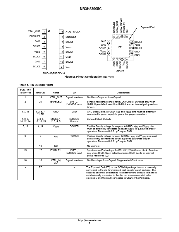
Click to expand full text
NB3H83905C 
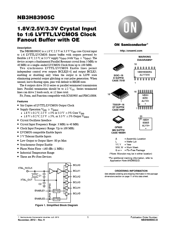
1.8V/2.5V/3.3V Crystal Input to 1:6 LVTTL/LVCMOS Clock Fanout Buffer with OE Description The NB3H83905C is a 1.8 V, 2.5 V or 3.3 V VDD core Crystal input to 1:6 LVTTL/LVCMOS fanout buffer with outputs powered by flexible 1.8 V, 2.5 V, or 3.3 V supply VDDO (with VDD w VDDO). The device accepts a fundamental Parallel Resonant crystal from 3 MHz to 40 MHz or a single−ended LVCMOS Clock from up to 100 MHz. 
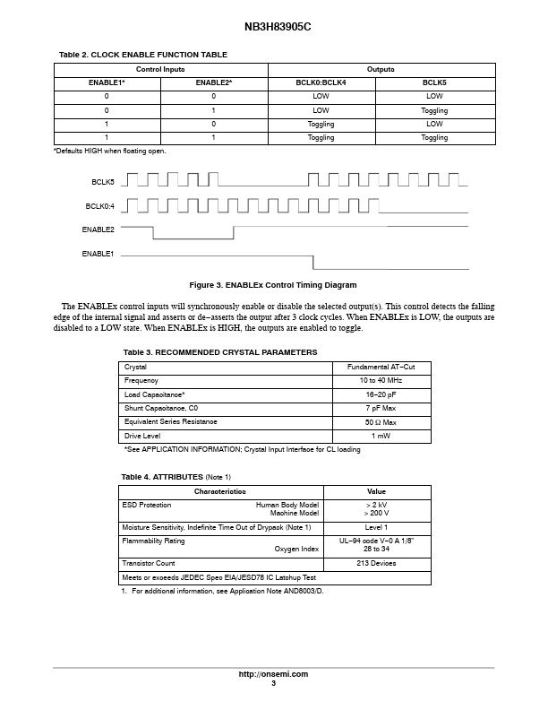
Two synchronous LVTTL/LVCMOS Enable lines permit independent control over outputs BCLK[0:4] and output BCLK5; enabling or disabling only when the output is in LOW state eliminating potential output glitching or runt pulse generation. When unused, leave floating open, pins will default to HIGH state. The 6 outputs drive 50 W series or parallel terminated transmission lines.
Published: |