Datasheet Details
| Part number | NB3F8L3010C |
|---|---|
| Manufacturer | ON Semiconductor |
| File Size | 110.40 KB |
| Description | 3.3V / 2.5V / 1.8V / 1.5V 3:1:10 LVCMOS Fanout Buffer |
| Datasheet |
 NB3F8L3010C Datasheet NB3F8L3010C Datasheet
|

|
|
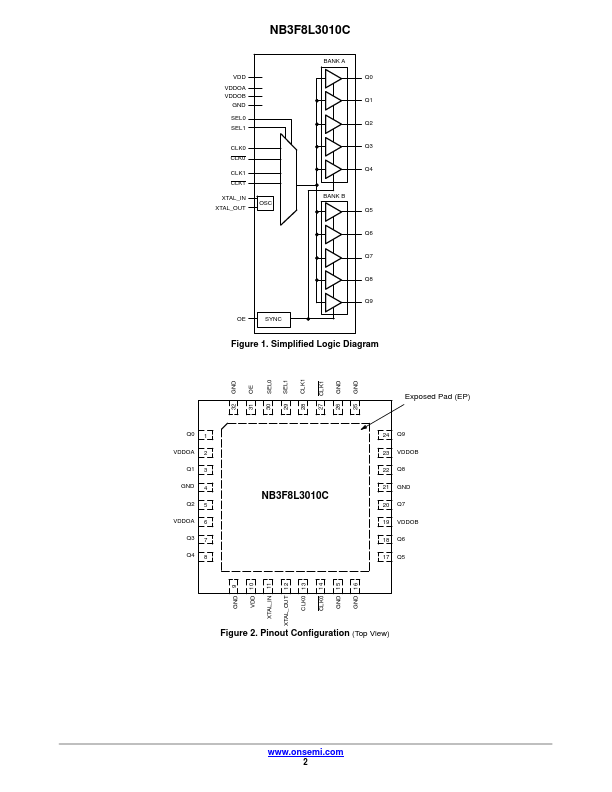
on a 3.3 V / 2.5 V Core VDD and two flexible 3.3 V / 2.5 V / 1.8 V / 1.5 V VDDOn supplies which must be equal or less than VDD.
A Mux selects between a Crystal input, or either of two differential/SE Clock / Data inputs.
| Part number | NB3F8L3010C |
|---|---|
| Manufacturer | ON Semiconductor |
| File Size | 110.40 KB |
| Description | 3.3V / 2.5V / 1.8V / 1.5V 3:1:10 LVCMOS Fanout Buffer |
| Datasheet |
NB3F8L3010C Datasheet
|
|
|
|