Datasheet Details
| Part number | NB3H63143G |
|---|---|
| Manufacturer | ON Semiconductor |
| File Size | 383.83 KB |
| Description | Programmable Clock Generator |
| Datasheet |
 NB3H63143G Datasheet NB3H63143G Datasheet
|
|
|
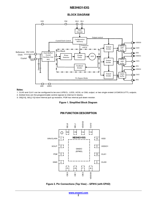
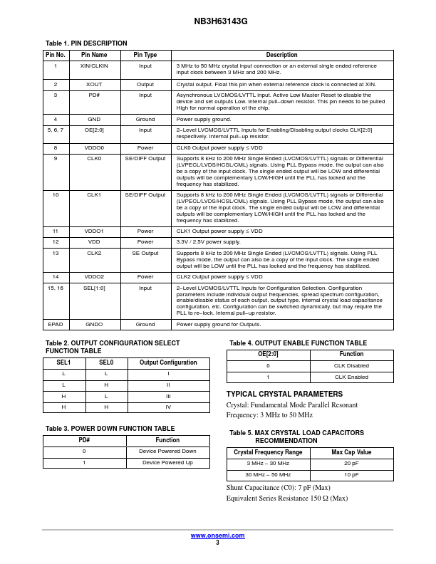
Figure 2.
Table 1.
Pin No.
| Part number | NB3H63143G |
|---|---|
| Manufacturer | ON Semiconductor |
| File Size | 383.83 KB |
| Description | Programmable Clock Generator |
| Datasheet |
NB3H63143G Datasheet
|
|
|
|