Datasheet Details
| Part number | NB100LVEP91 |
|---|---|
| Manufacturer | onsemi |
| File Size | 285.02 KB |
| Description | 2.5 V/3.3 V Any Level Positive Input to -2.5 V/-3.3 V LVNECL Output Translator |
| Datasheet |
 NB100LVEP91 Datasheet NB100LVEP91 Datasheet
|
|
|
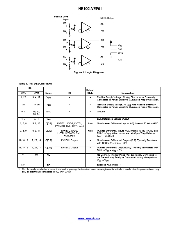
output translator.
2.5 V/3.3 V).
| Part number | NB100LVEP91 |
|---|---|
| Manufacturer | onsemi |
| File Size | 285.02 KB |
| Description | 2.5 V/3.3 V Any Level Positive Input to -2.5 V/-3.3 V LVNECL Output Translator |
| Datasheet |
NB100LVEP91 Datasheet
|
|
|
|