Datasheet Details
| Part number | NB100LVEP17 |
|---|---|
| Manufacturer | onsemi |
| File Size | 218.36 KB |
| Description | Quad Differential Driver/Receiver |
| Datasheet |
 NB100LVEP17 Datasheet NB100LVEP17 Datasheet
|
|
|
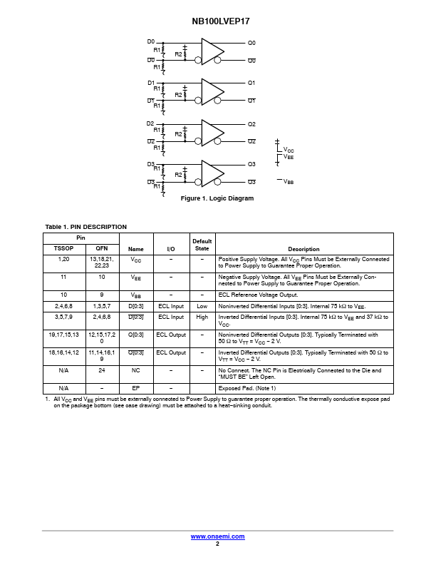
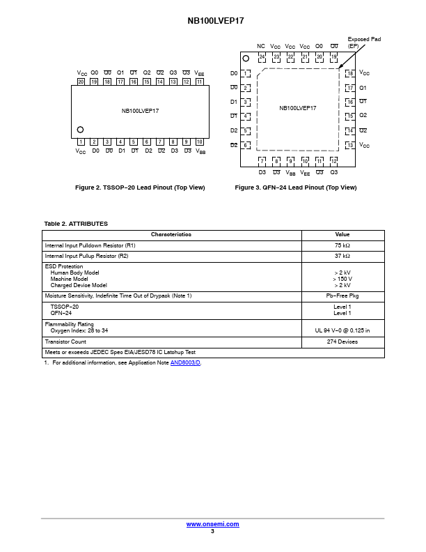
The NB100LVEP17 is a 4-bit differential line receiver.
incorporates two stages of gain, internal to the device, making it an excellent choice for use in high bandwidth amplifier applications.
The VBB pin, an internally generated voltage supply, is available to this device only.
| Part number | NB100LVEP17 |
|---|---|
| Manufacturer | onsemi |
| File Size | 218.36 KB |
| Description | Quad Differential Driver/Receiver |
| Datasheet |
NB100LVEP17 Datasheet
|
|
|
|