Datasheet4U Logo Datasheet4U.com

NB100LVEP222 - 1:15 Differential ECL/PECL /1 /2 Clock Driver

Description

PIN CLK0 , CLK0 CLK1 , CLK1 CLK_Sel MR Qa0:1, Qa0:1 Qb0:2, Qb0:2 Qc0:3, Qc0:3 Qd0:5, Qd0:5 fseln VBB VCC, VCC0 VEE NC FUNCTION ECL Differential Input Clock ECL Differential Input Clock ECL Clock Select ECL Master Reset ECL Differential Output

Features

  • C/VCC0. The VIHCMR range is referenced to the most positive side of the differential input signal. LVNECL DC.

📥 Download Datasheet

Datasheet preview – NB100LVEP222

Datasheet Details

Part number NB100LVEP222
Manufacturer onsemi
File Size 143.38 KB
Description 1:15 Differential ECL/PECL /1 /2 Clock Driver
Datasheet download datasheet NB100LVEP222 Datasheet
Additional preview pages of the NB100LVEP222 datasheet.
Other Datasheets by ON Semiconductor

Full PDF Text Transcription

Click to expand full text
NB100LVEP222 2.5 V/3.3 V 1:15 Differential ECL/PECL ÷1/÷2 Clock Driver 
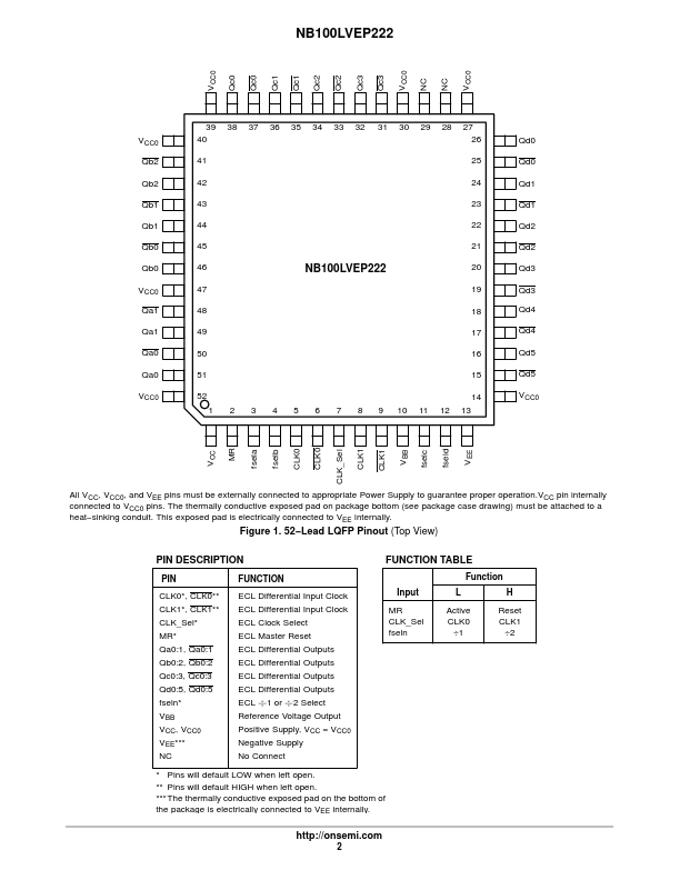
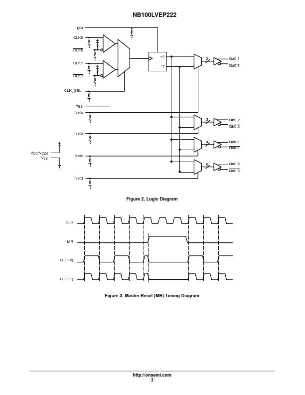
The NB100LVEP222 is a low skew 1:15 differential ÷1/÷2 ECL fanout buffer designed with clock distribution in mind. The LVECL/LVPECL input signal pairs can be used in a differential configuration or single−ended (with VBB output reference bypassed and connected to the unused input of a pair). Either of two fully differential clock inputs may be selected. Each of the four output banks of 2, 3, 4, and 6 differential pairs may be independently configured to fanout 1X or 1/2X of the input frequency. When the output banks are configured with the B1 mode, data can also be distributed. The LVEP222 specifically guarantees low output to output skew.
Published: |