Datasheet Details
| Part number | MC74VHC1GT03 |
|---|---|
| Manufacturer | onsemi |
| File Size | 166.18 KB |
| Description | 2-Input NOR Gate |
| Datasheet |
 MC74VHC1GT03 Datasheet MC74VHC1GT03 Datasheet
|
|
|
Download the MC74VHC1GT03 datasheet PDF. This datasheet also covers the MC74VHC1G03 variant, as both devices belong to the same 2-input nor gate family and are provided as variant models within a single manufacturer datasheet.
| Part number | MC74VHC1GT03 |
|---|---|
| Manufacturer | onsemi |
| File Size | 166.18 KB |
| Description | 2-Input NOR Gate |
| Datasheet |
MC74VHC1GT03 Datasheet
|
|
|
|
Note: Below is a high-fidelity text extraction (approx. 800 characters) for MC74VHC1GT03. For precise diagrams, and layout, please refer to the original PDF.
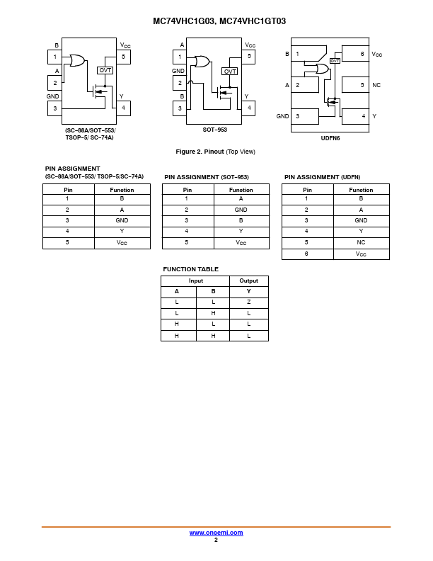
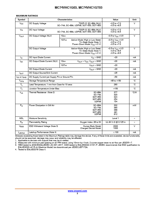
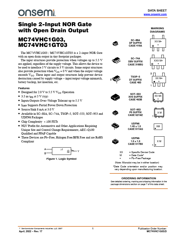
DATA SHEET www.onsemi.com Single 2-Input NOR Gate with Open Drain Output MC74VHC1G03, MC74VHC1GT03 The MC74VHC1G03 / MC74VHC1GT03 is a 2−input NOR Gate with an open drain...
| Part Number | Description |
|---|---|
| MC74VHC1GT00 | Single 2-Input NAND Gate |
| MC74VHC1GT01 | 2-Input NAND Gate |
| MC74VHC1GT02 | Single 2-Input NOR Gate |
| MC74VHC1GT04 | Single Inverter |
| MC74VHC1GT05 | Single Inverter |
| MC74VHC1GT07 | Single Non-Inverting Buffer |
| MC74VHC1GT08 | Single 2-Input AND Gate |
| MC74VHC1GT08E | Single 2-Input AND Gate |
| MC74VHC1GT125 | Noninverting 3-State Buffer |
| MC74VHC1GT126 | Noninverting 3-State Buffer |