Full PDF Text Transcription for MC74VHC1GT125 (Reference)
Note: Below is a high-fidelity text extraction (approx. 800 characters) for
MC74VHC1GT125. For precise diagrams, and layout, please refer to the original PDF.
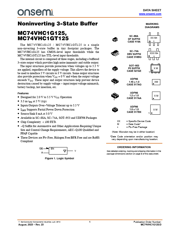
DATA SHEET www.onsemi.com Noninverting 3-State Buffer MC74VHC1G125, MC74VHC1GT125 The MC74VHC1G125 / MC74VHC1GT125 is a single non−inverting 3−state buffer in tiny footpr...
View more extracted text
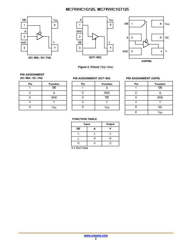
MC74VHC1GT125 is a single non−inverting 3−state buffer in tiny footprint packages. The MC74VHC1G125 has CMOS−level input thresholds while the MC74VHC1GT125 has TTL−level input thresholds. The internal circuit is composed of three stages, including a buffered 3−state output which provides high noise immunity and stable output. The input structures provide protection when voltages up to 5.5 V are applied, regardless of the supply voltage. This allows the device to be used to interface 5 V circuits to 3 V circuits. Some output structures also provide protection when VCC = 0 V and when the output voltage exceeds VCC.
 MC74VHC1GT125 Datasheet