Datasheet Details
| Part number | MC100LVEL34 |
|---|---|
| Manufacturer | onsemi |
| File Size | 91.99 KB |
| Description | Clock Generation Chip |
| Datasheet |
 MC100LVEL34 Datasheet MC100LVEL34 Datasheet
|
|
|
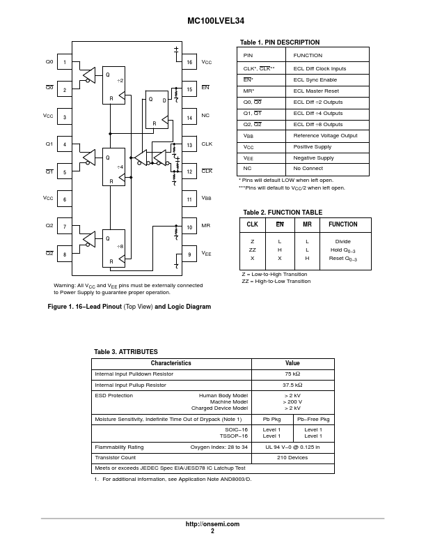
chip designed explicitly for low skew clock generation applications.
The internal dividers are synchronous to each other, therefore, the common output edges are all precisely aligned.
| Part number | MC100LVEL34 |
|---|---|
| Manufacturer | onsemi |
| File Size | 91.99 KB |
| Description | Clock Generation Chip |
| Datasheet |
MC100LVEL34 Datasheet
|
|
|
|
Note: Below is a high-fidelity text extraction (approx. 800 characters) for MC100LVEL34. For precise diagrams, and layout, please refer to the original PDF.
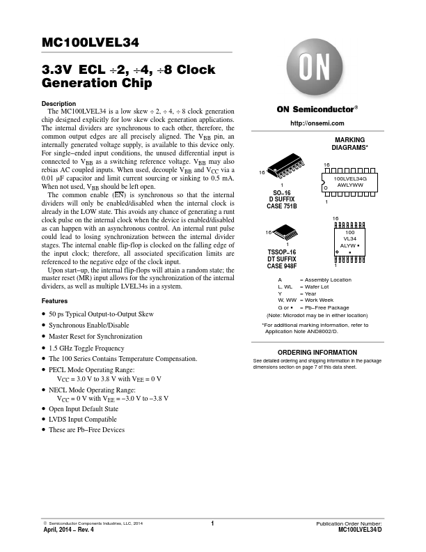
MC100LVEL34 3.3V ECL ÷2, ÷4, ÷8 Clock Generation Chip Description The MC100LVEL34 is a low skew ÷ 2, ÷ 4, ÷ 8 clock generation chip designed explicitly for low skew clock...
| Part Number | Description |
|---|---|
| MC100LVEL30 | Triple D Flip-Flop |
| MC100LVEL31 | 3.3V ECL D Flip?Flop |
| MC100LVEL32 | 2 Divider |
| MC100LVEL33 | Divider |
| MC100LVEL37 | Clock Fanout Buffer |
| MC100LVEL38 | Clock Generation Chip |
| MC100LVEL39 | Clock Generation Chip |
| MC100LVEL01 | 4-Input OR/NOR |
| MC100LVEL05 | 2-Input Differential AND/NAND |
| MC100LVEL11 | Low Voltage 1:2 Differential Fanout Buffer |