Download the BS107 datasheet PDF.
This datasheet also covers the BS107A variant, as both devices belong to the same small signal mosfet family and are provided as variant models within a single manufacturer datasheet.
Note: Below is a high-fidelity text extraction (approx. 800 characters) for
BS107. For precise diagrams, and layout, please refer to the original PDF.
www.DataSheet4U.com BS107, BS107A Preferred Device Small Signal MOSFET 250 mAmps, 200 Volts N–Channel TO–92 MAXIMUM RATINGS Rating Drain–Source Voltage Gate–Source Voltag...
View more extracted text
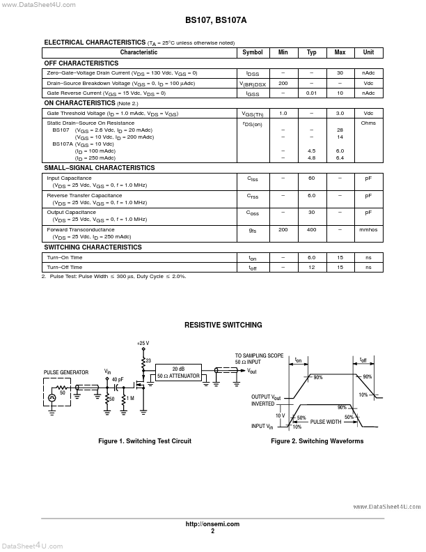
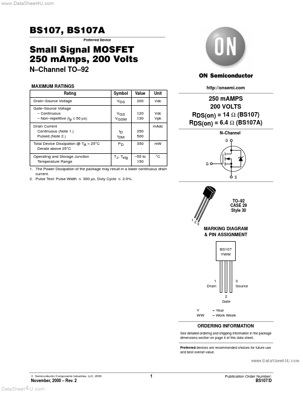
l TO–92 MAXIMUM RATINGS Rating Drain–Source Voltage Gate–Source Voltage – Continuous – Non–repetitive (tp ≤ 50 µs) Drain Current Continuous (Note 1.) Pulsed (Note 2.) Total Device Dissipation @ TA = 25°C Derate above 25°C Operating and Storage Junction Temperature Range Symbol VDS VGS VGSM ID IDM PD TJ, Tstg Value 200 ±20 ±30 250 500 350 –55 to 150 mW °C G S Unit Vdc Vdc Vpk mAdc http://onsemi.com 250 mAMPS 200 VOLTS RDS(on) = 14 Ω (BS107) RDS(on) = 6.4 Ω (BS107A) N–Channel D 1. The Power Dissipation of the package may result in a lower continuous drain current. 2. Pulse Test: Pulse Width v 300 µs, Duty Cycle v 2.0%.
 BS107 Datasheet