Note: Below is a high-fidelity text extraction (approx. 800 characters) for
BF422. For precise diagrams, and layout, please refer to the original PDF.
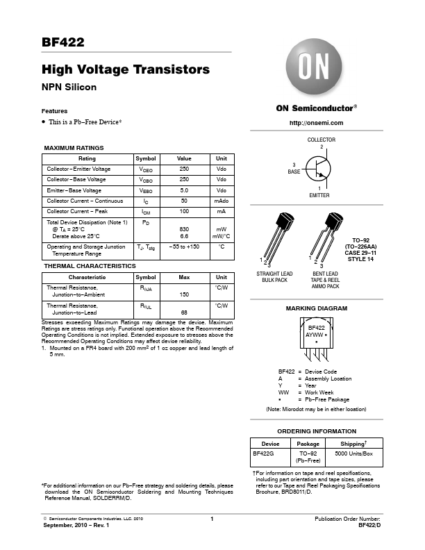
BF422 High Voltage Transistors NPN Silicon Features • This is a Pb−Free Device* MAXIMUM RATINGS Rating Collector −Emitter Voltage Collector −Base Voltage Emitter−Base Vol...
View more extracted text
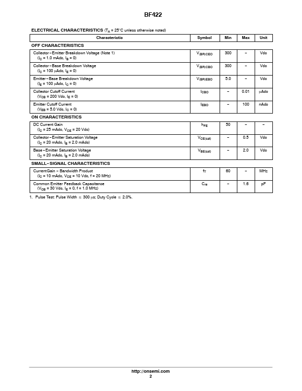
ng Collector −Emitter Voltage Collector −Base Voltage Emitter−Base Voltage Collector Current − Continuous Collector Current − Peak Total Device Dissipation (Note 1) @ TA = 25°C Derate above 25°C Operating and Storage Junction Temperature Range Symbol VCEO VCBO VEBO IC ICM PD TJ, Tstg Value 250 250 5.0 50 100 830 6.6 −55 to +150 Unit Vdc Vdc Vdc mAdc mA mW mW/°C °C THERMAL CHARACTERISTICS Characteristic Thermal Resistance, Junction−to−Ambient Symbol RqJA Max 150 Unit °C/W Thermal Resistance, Junction−to−Lead RqJL °C/W 68 Stresses exceeding Maximum Ratings may damage the device. Maximum Ratings are stress ratings only.
 BF422 Datasheet