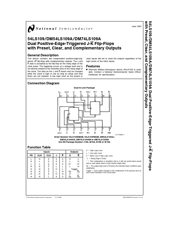
This device contains two independent positive-edge-triggered J-K flip-flops with complementary outputs The J and K data is accepted by the flip-flop on the rising edge of the clock pulse The triggering occurs at a voltage level and is not directly related to the transition time of the rising edge of
Key Features
Y
Alternate Military Aerospace device (54LS109) is available Contact a National Semiconductor Sales Office Distributor for specifications
Connection Diagram
Dual-In-Line Package
TL F 6368.
1
Order Number 54LS109DMQB 54LS109FMQB DM54LS109AJ DM54LS109AW DM74LS109AM or DM74LS109AN See NS Package Number J16A M16A N16E or W16A
Function Table
Inputs PR L H L H H H H H CLR H L L H H H H H CLK X X X J X X X L H L H X K X X X L L H H X Outputs Q H L H L Q
H e High Logic Level L e Low Logic.
Full PDF Text Transcription for DM74LS109A (Reference)
Note: Below is a high-fidelity text extraction (approx. 800 characters) for
DM74LS109A. For precise diagrams, and layout, please refer to the original PDF.
54LS109 DM54LS109A DM74LS109A Dual Positive-Edge-Triggered J-K Flip-Flops with Preset Clear and Complementary Outputs June 1989 54LS109 DM54LS109A DM74LS109A Dual Positiv...
View more extracted text
lementary Outputs June 1989 54LS109 DM54LS109A DM74LS109A Dual Positive-Edge-Triggered J-K Flip-Flops with Preset Clear and Complementary Outputs General Description This device contains two independent positive-edge-triggered J-K flip-flops with complementary outputs The J and K data is accepted by the flip-flop on the rising edge of the clock pulse The triggering occurs at a voltage level and is not directly related to the transition time of the rising edge of the clock The data on the J and K inputs may be changed while the clock is high or low as long as setup and hold times are not violated A low logic level on the pr
 DM74LS109A Datasheet