Datasheet Details
| Part number | SSTUH32864 |
|---|---|
| Manufacturer | NXP Semiconductors |
| File Size | 142.46 KB |
| Description | 1.8 V high output drive configurable registered buffer |
| Datasheet |
 SSTUH32864 Datasheet SSTUH32864 Datasheet
|
|
|
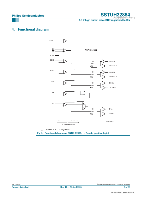
The SSTUH32864 is a 25-bit 1 : 1 or 14-bit 1 : 2 configurable registered buffer designed for 1.7 V to 1.9 V VDD operation.
All clock and data inputs are compatible with the JEDEC standard for SSTL_18.
The control inputs are LVCMOS.
| Part number | SSTUH32864 |
|---|---|
| Manufacturer | NXP Semiconductors |
| File Size | 142.46 KB |
| Description | 1.8 V high output drive configurable registered buffer |
| Datasheet |
SSTUH32864 Datasheet
|
|
|
|
| Part Number | Description | Manufacturer |
|---|---|---|
| SST108 | N-Channel JFET Switch | Calogic |
| SST108 | Switching | Micross |
| SST108 | N-Channel JFETs | Vishay |
| SST109 | N-Channel JFET Switch | Calogic |
| SST109 | Switching | Micross |
| Part Number | Description |
|---|---|
| SSTUH32865 | 1.8V 28-bit high output drive 1:2 registered buffer |
| SSTUH32866 | 1.8 V high output drive 25-bit 1 : 1 or 14-bit 1 : 2 configurable registered buffer |
| SSTU32864 | 1.8V confgurable registered buffer |
| SSTU32865 | 28-bit 1:2 registered buffer |
| SSTU32866 | 1.8V 25-bit 1:1 or 14-bit 1:2 confgurable registered buffer |
The following content is an automatically extracted verbatim text from the original manufacturer datasheet and is provided for reference purposes only.