Datasheet Details
| Part number | SSTU32866 |
|---|---|
| Manufacturer | NXP Semiconductors |
| File Size | 177.95 KB |
| Description | 1.8V 25-bit 1:1 or 14-bit 1:2 confgurable registered buffer |
| Datasheet |
 SSTU32866 Datasheet SSTU32866 Datasheet
|
|
|
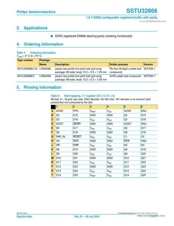
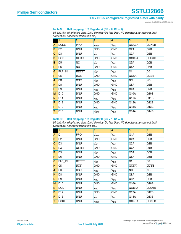
The SSTU32866 is a 1.8 V configurable register specifically designed for use on DDR2 memory modules requiring a parity checking function.
It is defined in accordance with the JEDEC JESD82-7 standard for the SSTU32864 registered buffer, while adding the parity checking function in a compatible pinout.
| Part number | SSTU32866 |
|---|---|
| Manufacturer | NXP Semiconductors |
| File Size | 177.95 KB |
| Description | 1.8V 25-bit 1:1 or 14-bit 1:2 confgurable registered buffer |
| Datasheet |
SSTU32866 Datasheet
|
|
|
|
| Part Number | Description | Manufacturer |
|---|---|---|
| SST108 | N-Channel JFET Switch | Calogic |
| SST108 | Switching | Micross |
| SST108 | N-Channel JFETs | Vishay |
| SST109 | N-Channel JFET Switch | Calogic |
| SST109 | Switching | Micross |
| Part Number | Description |
|---|---|
| SSTU32864 | 1.8V confgurable registered buffer |
| SSTU32865 | 28-bit 1:2 registered buffer |
| SSTUA32864 | configurable registered buffer |
| SSTUA32866 | configurable registered buffer |
| SSTUB32866 | configurable registered buffer |
The following content is an automatically extracted verbatim text from the original manufacturer datasheet and is provided for reference purposes only.