Click to expand full text
INTEGRATED CIRCUITS
DATA SHEET
74LVC2G34 Dual buffer gate
Product specification Supersedes data of 2003 Jul 25 2004 Sep 10
Philips Semiconductors
Product specification
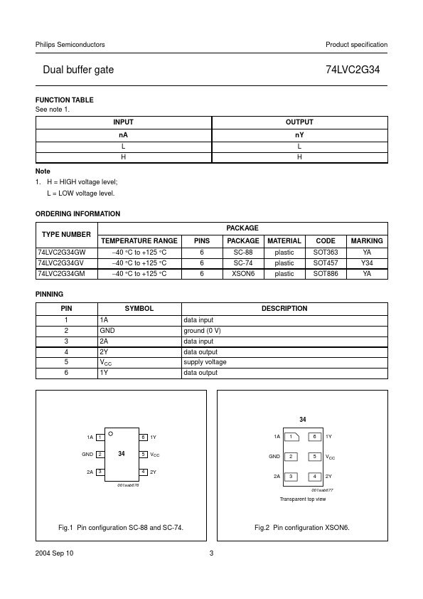
Dual buffer gate
FEATURES • Wide supply voltage range from 1.65 V to 5.5 V • 5 V tolerant input/output for interfacing with 5 V logic • High noise immunity • Complies with JEDEC standard: – JESD8-7 (1.65 V to 1.95 V) – JESD8-5 (2.3 V to 2.7 V) – JESD8B/JESD36 (2.7 V to 3.6 V). • ESD protection: – HBM EIA/JESD22-A114-B exceeds 2000 V – MM EIA/JESD22-A115-A exceeds 200 V. • ±24 mA output drive (VCC = 3.0 V) • CMOS low power consumption • Latch-up performance exceeds 250 mA • Direct interface with TTL levels • Multiple package options • Specified from −40 °C to +85 °C and −40 °C to +125 °C.
 74LVC2G34 Datasheet