Datasheet Details
| Part number | NX3V1T66 |
|---|---|
| Manufacturer | NXP Semiconductors |
| File Size | 170.23 KB |
| Description | Low-voltage analog switch |
| Datasheet |
 NX3V1T66 Datasheet NX3V1T66 Datasheet
|
|
|
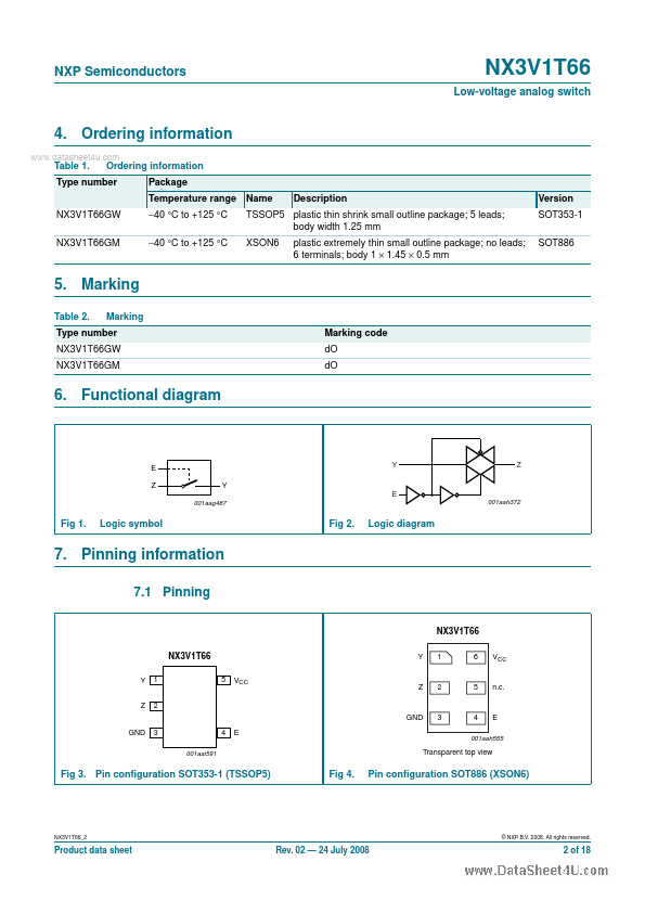
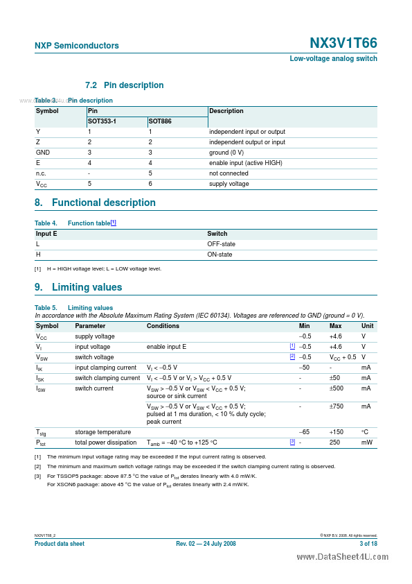
The NX3V1T66 provides one single-pole single-throw analog switch function.
It has two input/output terminals (Y and Z) and an active HIGH enable input pin (E).
When pin E is LOW, the analog switch is turned off.
| Part number | NX3V1T66 |
|---|---|
| Manufacturer | NXP Semiconductors |
| File Size | 170.23 KB |
| Description | Low-voltage analog switch |
| Datasheet |
NX3V1T66 Datasheet
|
|
|
|
| Part Number | Description | Manufacturer |
|---|---|---|
| NX3V1T384 | Low-ohmic Single-pole Single-throw Analog Switch | NXP |
| NX3008CBKS | N/P-channel MOSFET | nexperia |
| NX3008CBKV | N/P-channel MOSFET | nexperia |
| NX3008NBK | N-channel MOSFET | nexperia |
| NX3008NBK | MOSFET | NXP |
| Part Number | Description |
|---|---|
| NX3V1G384 | Low-ohmic single-pole single-throw analog switch |
| NX3V1G66 | Low-voltage analog switch |
| NX3008CBKS | MOSFET |
| NX3008CBKV | MOSFET |
| NX3008NBKMB | MOSFET |
The following content is an automatically extracted verbatim text from the original manufacturer datasheet and is provided for reference purposes only.