Click to expand full text
NIKO-SEM
N-Channel Enhancement Mode
P0920ATF
Field Effect Transistor
TO-220F
Halogen-Free & Lead-Free
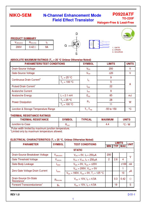
PRODUCT SUMMARY
V(BR)DSS
RDS(ON)
200V
0.42Ω
ID 9A
D G
S
ABSOLUTE MAXIMUM RATINGS (TA = 25 °C Unless Otherwise Noted)
PARAMETERS/TEST CONDITIONS
SYMBOL
Drain-Source Voltage Gate-Source Voltage Continuous Drain Current2 Pulsed Drain Current1 Avalanche Current Avalanche Energy
Power Dissipation
Junction & Storage Temperature Range
TC = 25 °C TC = 100 °C
L = 2.1 mH TC = 25 °C TC = 100 °C
VDS VGS
ID
IDM IAS EAS PD
TJ, Tstg
THERMAL RESISTANCE RATINGS THERMAL RESISTANCE
SYMBOL
Junction-to-Case
RJC
1Pulse width limited by maximum junction temperature. 2Limited only by maximum temperature allowed.
TYPICAL
1 23
1. GATE 2. DRAIN 3.
 P0920ATF Datasheet