The following content is an automatically extracted verbatim text
from the original manufacturer datasheet and is provided for reference purposes only.
View original datasheet text
SMD Type
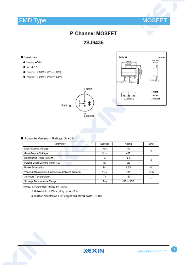
P-Channel MOSFET 2SJ9435
TraMnOsiSsFtoErsT
■ Features
● VDS (V) =-30V ● ID =-4.2 A ● RDS(ON) < 50mΩ (VGS =-10V) ● RDS(ON) < 90mΩ (VGS =-4.5V)
1.Gate
2.Drain 3.Source
1.70 0.1
0.42 0.1
0.46 0.1
1.Gate 2.Drain 3.Source
■ Absolute Maximum Ratings (Ta = 25℃)
Parameter Drain-Source Voltage Gate-Source Voltage Continuous Drain Current Pulsed Drain Current (Note 1, 2) Power Dissipation Thermal Resistance.Junction- to-Ambient (Note 3) Junction Temperature Storage Temperature Range
Symbol VDS VGS ID IDM PD RthJA TJ Tstg
Notes: 1. Pulse width limited by TJ(MAX) 2. Pulse width ≤300µs , duty cycle ≤2%. 3: Surface mounted on 1 in 2 copper pad of FR4 board, t ≤10s.
Rating -30 ±20 -4.2 -20 1.25 100 150
-55 to 150
Unit V
A W ℃/W ℃
www.kexin.com.
 2SJ9435 Datasheet