Datasheet Details
| Part number | 8V44N4614 |
|---|---|
| Manufacturer | Integrated Device Technology |
| File Size | 593.68 KB |
| Description | NG Jitter Attenuator and Clock Synthesizer |
| Datasheet |
 8V44N4614 Datasheet 8V44N4614 Datasheet
|
|
|
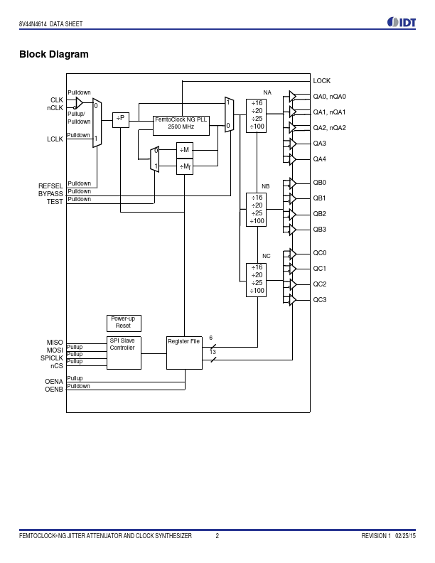
The 8V44N4614 is a FemtoClock® NG Clock Generator.
The device has been designed for frequency generation in high-performance systems such wireless base-band boards, for instance to drive the reference clock inputs of processors, PHY, switch and SerDes devices.
| Part number | 8V44N4614 |
|---|---|
| Manufacturer | Integrated Device Technology |
| File Size | 593.68 KB |
| Description | NG Jitter Attenuator and Clock Synthesizer |
| Datasheet |
8V44N4614 Datasheet
|
|
|
|