Datasheet4U Logo Datasheet4U.com

ICS86953I-147 - 1-TO-9 DIFFERENTIAL-TO-LVCMOS / LVTTL ZERO DELAY BUFFER

Description

The ICS86953I-147 is a low voltage, low skew 1-to-9 Differential-to-LVCMOS/LVTTL Clock HiPerClockS™ Generator and a member of the HiPerClock S ™ family of High Performance Clock Solutions from ICS.

The PCLK, nPCLK pair can accept most standard differential input levels.

Features

  • 9 single ended LVCMOS/LVTTL outputs; (8) clocks, (1) feedback.
  • PCLK, nPCLK pair can accept the following differential input levels: LVPECL, CML, SSTL.
  • Maximum output frequency: PLL Mode, 175MHz.
  • VCO range: 250MHz to 700MHz.
  • Output skew: 75ps (maximum).
  • Cycle-to-cycle jitter: 50ps (maximum).
  • Static phase offset: 90ps ± 110ps.
  • 3.3V supply voltage.

📥 Download Datasheet

Datasheet Details

Part number ICS86953I-147
Manufacturer Integrated Circuit Systems
File Size 291.86 KB
Description 1-TO-9 DIFFERENTIAL-TO-LVCMOS / LVTTL ZERO DELAY BUFFER
Datasheet download datasheet ICS86953I-147 Datasheet

Full PDF Text Transcription

Click to expand full text
Integrated Circuit Systems, Inc.
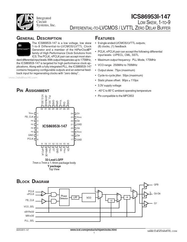
 ICS86953I-147 LOW SKEW, 1-TO-9 DIFFERENTIAL-TO-LVCMOS / LVTTL ZERO DELAY BUFFER FEATURES • 9 single ended LVCMOS/LVTTL outputs; (8) clocks, (1) feedback • PCLK, nPCLK pair can accept the following differential input levels: LVPECL, CML, SSTL • Maximum output frequency: PLL Mode, 175MHz • VCO range: 250MHz to 700MHz • Output skew: 75ps (maximum) • Cycle-to-cycle jitter: 50ps (maximum) • Static phase offset: 90ps ± 110ps • 3.3V supply voltage GENERAL DESCRIPTION The ICS86953I-147 is a low voltage, low skew 1-to-9 Differential-to-LVCMOS/LVTTL Clock HiPerClockS™ Generator and a member of the HiPerClock S ™ family of High Performance Clock Solutions from ICS. The PCLK, nPCLK pair can accept most standard differential input levels.
Published: |