Click to expand full text
128K X 36, 3.3V Synchronous IDT71V547S/XS SRAM with ZBT™ Feature, Burst Counter and Flow-Through Outputs
Features
◆ 128K x 36 memory configuration, flow-through outputs ◆ Supports high performance system speed - 95 MHz
(8ns Clock-to-Data Access) ◆ ZBTTM Feature - No dead cycles between write and read
cycles ◆ Internally synchronized signal eliminates the need to
control OE
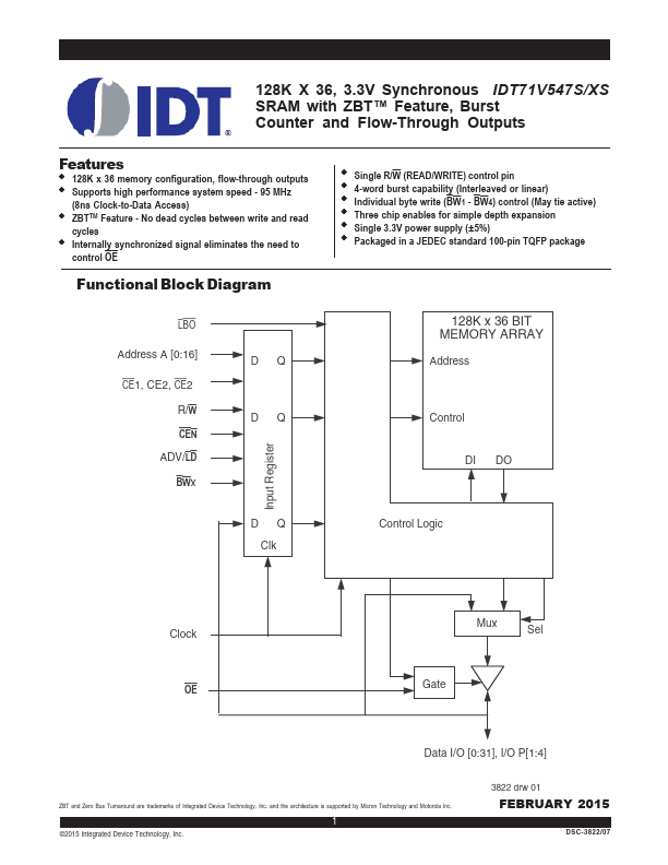
Functional Block Diagram
LBO
Address A [0:16]
CE1, CE2, CE2 R/W CEN
ADV/LD BWx
DQ DQ
◆ Single R/W (READ/WRITE) control pin ◆ 4-word burst capability (Interleaved or linear) ◆ Individual byte write (BW1 - BW4) control (May tie active) ◆ Three chip enables for simple depth expansion ◆ Single 3.
 IDT71V547XS Datasheet