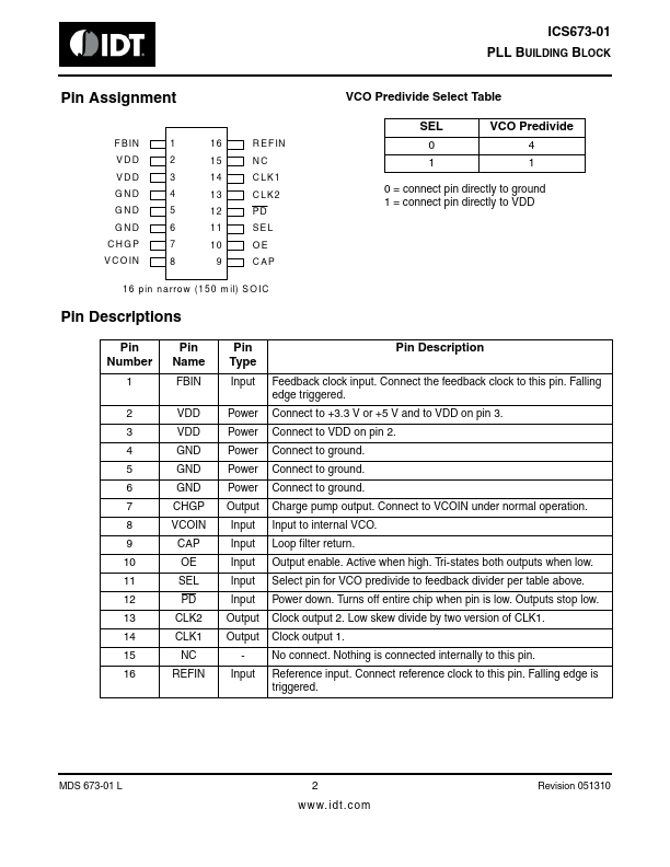
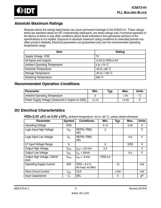
Datasheet Details
| Part number | ICS673-01 |
|---|---|
| Manufacturer | IDT |
| File Size | 84.03 KB |
| Description | PLL BUILDING BLOCK |
| Datasheet |
 ICS673-01 Datasheet ICS673-01 Datasheet
|
|
|
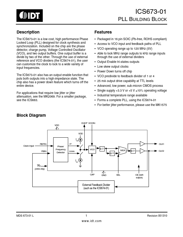
The ICS673-01 is a low cost, high performance Phase Locked Loop (PLL) designed for clock synthesis and synchronization.
Included on the chip are the phase detector, charge pump, Voltage Controlled Oscillator (VCO), and two output buffers.
One output buffer is a divide by two of the other.
| Part number | ICS673-01 |
|---|---|
| Manufacturer | IDT |
| File Size | 84.03 KB |
| Description | PLL BUILDING BLOCK |
| Datasheet |
ICS673-01 Datasheet
|
|
|
|