Click to expand full text
HY5RS573225F
www.DataSheet4U.com
256M (8Mx32) GDDR3 SDRAM HY5RS573225F
This document is a general product description and is subject to change without notice. Hynix Electronics does not assume any responsibility for use of circuits described. No patent licenses are implied. Rev. 0.4 / Apr. 2004 1
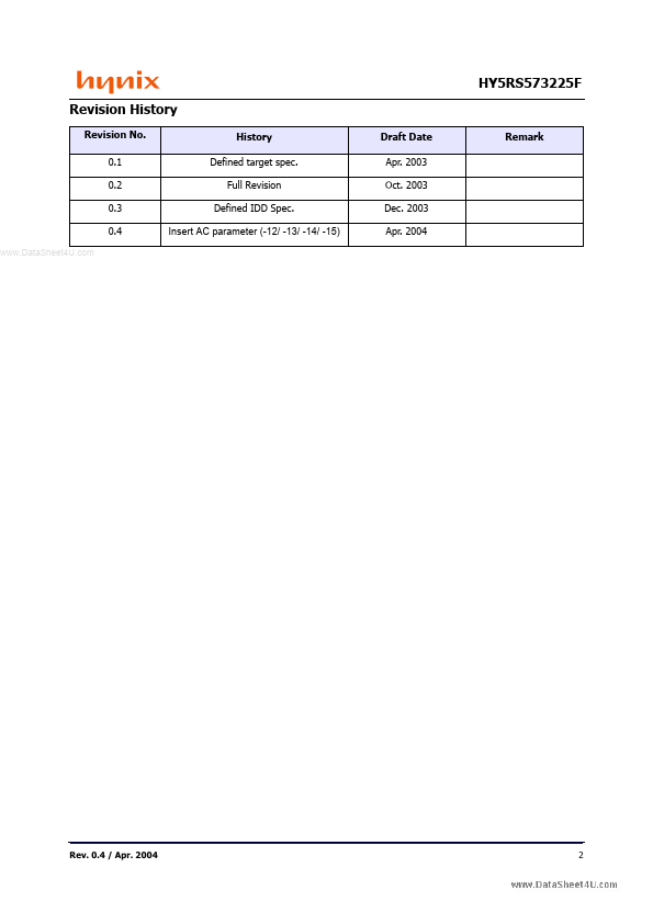
HY5RS573225F Revision History
Revision No. 0.1 0.2 0.3 0.4
www.DataSheet4U.com
History Defined target spec. Full Revision Defined IDD Spec. Insert AC parameter (-12/ -13/ -14/ -15)
Draft Date Apr. 2003 Oct. 2003 Dec. 2003 Apr. 2004
Remark
Rev. 0.4 / Apr. 2004
2
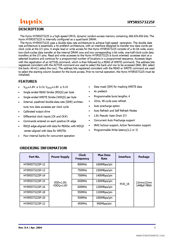
HY5RS573225F DESCRIPTION
The Hynix HY5RS573225 is a high-speed CMOS, dynamic random-access memory containing 268,435,456 bits. The Hynix HY5RS573225 is internally configured as a quad-bank DRAM.
 HY5RS573225F Datasheet