Datasheet Details
| Part number | HY5RS123235BFP |
|---|---|
| Manufacturer | SK Hynix |
| File Size | 1.02 MB |
| Description | 512Mbit GDDR3 SDRAM |
| Datasheet |
 HY5RS123235BFP Datasheet HY5RS123235BFP Datasheet
|
|
|
and is subject to change without notice.
responsibility for use of circuits described.
No patent licenses are implied.
| Part number | HY5RS123235BFP |
|---|---|
| Manufacturer | SK Hynix |
| File Size | 1.02 MB |
| Description | 512Mbit GDDR3 SDRAM |
| Datasheet |
HY5RS123235BFP Datasheet
|
|
|
|
| Part Number | Description | Manufacturer |
|---|---|---|
| HY5-P | Current Transducers HY 5 to 25-P | LEM |
| HY50-P | Current Transducer HY 50-P | LEM |
| HY5002 | 1-chip composed of high-current totem pole | HAWYANG |
| HY5012A | N-Channel Enhancement Mode MOSFET | HOOYI |
| HY5012W | N-Channel Enhancement Mode MOSFET | HOOYI |
| Part Number | Description |
|---|---|
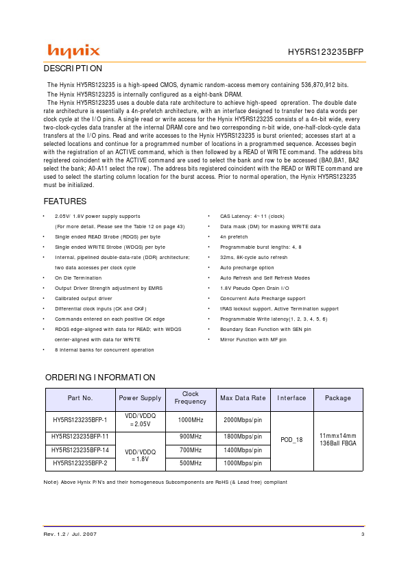
| HY5RS123235FP | 512M (16Mx32) GDDR3 SDRAM |
| HY5RS123235FP-11 | 512M (16Mx32) GDDR3 SDRAM |
| HY5RS123235FP-12 | 512M (16Mx32) GDDR3 SDRAM |
| HY5RS123235FP-14 | 512M (16Mx32) GDDR3 SDRAM |
| HY5RS123235FP-16 | 512M (16Mx32) GDDR3 SDRAM |