Datasheet Details
| Part number | HY5DU12422B |
|---|---|
| Manufacturer | SK Hynix |
| File Size | 407.17 KB |
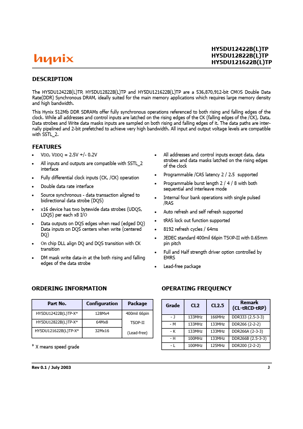
| Description | 512 Mb DDR SDRAM |
| Datasheet |
 HY5DU12422B Datasheet HY5DU12422B Datasheet
|
|
|
Download the HY5DU12422B datasheet PDF. This datasheet also covers the HY5DU121622 variant, as both devices belong to the same 512 mb ddr sdram family and are provided as variant models within a single manufacturer datasheet.
and is subject to change without notice.
Hynix semiconductor does not assume any responsibility for use of circuits described.
No patent licenses are implied.
| Part number | HY5DU12422B |
|---|---|
| Manufacturer | SK Hynix |
| File Size | 407.17 KB |
| Description | 512 Mb DDR SDRAM |
| Datasheet |
HY5DU12422B Datasheet
|
|
|
|
| Part Number | Description | Manufacturer |
|---|---|---|
| HY5DU281622 | 4 Banks x 2M x 16Bit Double Data Rate SDRAM | Hyundai |
| HY5DU281622FTP | 128Mb DDR SDRAM | Hynix |
| HY5DU281622LT-H | 4 Banks x 2M x 16Bit Double Data Rate SDRAM | Hyundai |
| HY5DU281622LT-K | 4 Banks x 2M x 16Bit Double Data Rate SDRAM | Hyundai |
| HY5DU281622LT-L | 4 Banks x 2M x 16Bit Double Data Rate SDRAM | Hyundai |
| Part Number | Description |
|---|---|
| HY5DU12422ALT | 512Mb DDR SDRAM |
| HY5DU12422AT | 512Mb DDR SDRAM |
| HY5DU12422C | 512 Mb DDR SDRAM |
| HY5DU121622ALT | 512Mb DDR SDRAM |
| HY5DU121622AT | 512Mb DDR SDRAM |