High speed switching
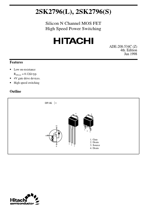
Outline
DPAK |1
D G
S
ADE-208-534C (Z) 4th. Edition Jun 1998
44
12 3
12 3
1. Gate 2. Drain 3. Source 4. Drain
2SK2796(L), 2SK2796(S)
Absolute Maximum Ratings (Ta = 25°C)
Item
Symbol
Drain to source voltage Gate to source voltage Drain current Drain peak current Body-drain diode reverse drain current Avalanche current Avalanche energy Channel dissipation
VDSS VGSS ID I Note1.
Note: Below is a high-fidelity text extraction (approx. 800 characters) for
K2796. For precise diagrams, and layout, please refer to the original PDF.
2SK2796(L), 2SK2796(S) Silicon N Channel MOS FET High Speed Power Switching Features • Low on-resistance RDS(on) = 0.12Ω typ. • 4V gate drive devices. • High speed switch...
View more extracted text
ance RDS(on) = 0.12Ω typ. • 4V gate drive devices. • High speed switching Outline DPAK |1 D G S ADE-208-534C (Z) 4th. Edition Jun 1998 44 12 3 12 3 1. Gate 2. Drain 3. Source 4. Drain 2SK2796(L), 2SK2796(S) Absolute Maximum Ratings (Ta = 25°C) Item Symbol Drain to source voltage Gate to source voltage Drain current Drain peak current Body-drain diode reverse drain current Avalanche current Avalanche energy Channel dissipation VDSS VGSS ID I Note1 D(pulse) I DR I Note3 AP E Note3 AR Pch Note2 Channel temperature Tch Storage temperature Tstg Note: 1. PW ≤ 10µs, duty cycle ≤ 1 % 2. Value at Tc = 25°C 3. Value at Tch = 25°C, R
More Datasheets from Hitachi Semiconductor (now Renesas)
 K2796 Datasheet