Description
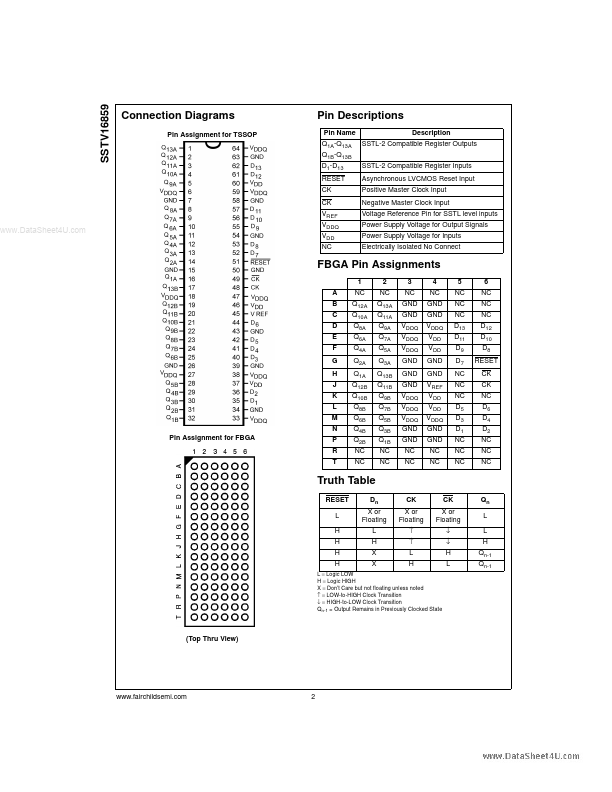
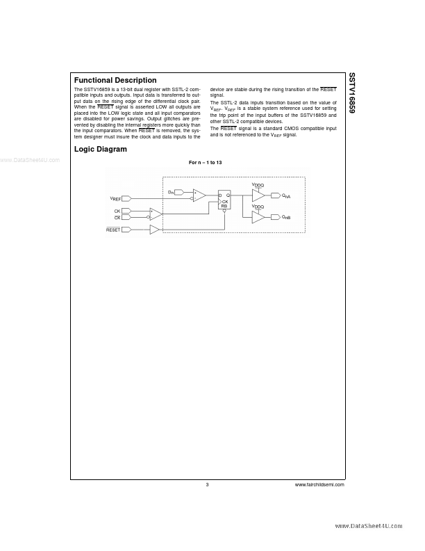
The SSTV16859 is a dual output 13-bit register designed for use with 184 and 232 pin DDR-1 memory modules.
The device has a differential input clock, SSTL-2 compatible data inputs and a LVCMOS compatible RESET input.
Features
- I Compliant with DDR-I registered module specifications I Operates at 2.5V ± 0.2V VDD I SSTL-2 compatible input structure I SSTL-2 compliant output structure I Differential SSTL-2 compatible clock inputs I Low power mode when device is reset I Industry standard 64 pin TSSOP package I Also packaged in plastic Fine-Pitch Ball Grid Array (FBGA)
Ordering Code:
Order Number SSTV16859G (Note 1)(Note 2) SSTV16859MTD (Note 2) Package Number BGA96A MTD64 Package.
 SSTV16859 Datasheet