Datasheet Details
| Part number | 74VCX162839 |
|---|---|
| Manufacturer | Fairchild (now onsemi) |
| File Size | 101.26 KB |
| Description | Low Voltage 20-Bit Selectable Register/Buffer |
| Datasheet |
 74VCX162839 Datasheet 74VCX162839 Datasheet
|
|
|
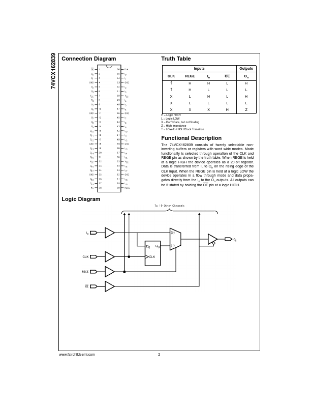
The VCX162839 contains twenty non-inverting selectable buffered or registered paths.
The device can be configured to operate in a registered, or flow through buffer mode by utilizing the register enable (REGE) and Clock (CLK) signals.
The device operates in a 20-bit word wide mode.
| Part number | 74VCX162839 |
|---|---|
| Manufacturer | Fairchild (now onsemi) |
| File Size | 101.26 KB |
| Description | Low Voltage 20-Bit Selectable Register/Buffer |
| Datasheet |
74VCX162839 Datasheet
|
|
|
|
| Part Number | Description | Manufacturer |
|---|---|---|
| 74VCX162244 | LOW VOLTAGE CMOS 16-BIT BUS BUFFER | ST Microelectronics |
| 74VCX16240 | LOW VOLTAGE CMOS 16-BIT BUS BUFFER | STMicroelectronics |
| 74VCX16240 | Low-Voltage 1.8/2.5/3.3V 16-Bit Buffer | ON Semiconductor |
| 74VCX16244 | Low-Voltage 1.8V/2.5V/3.3V 16-Bit Buffer | ON Semiconductor |
| 74VCX16245 | Low-Voltage 1.8/2.5/3.3V 16-Bit Transceiver | ON Semiconductor |
| Part Number | Description |
|---|---|
| 74VCX162835 | Low Voltage 18-Bit Universal Bus Driver |
| 74VCX162838 | Low Voltage 16-Bit Selectable Register/Buffer |
| 74VCX162827 | Low Voltage 20-Bit Buffer/Line Driver |
| 74VCX162240 | Low Voltage 16-Bit Inverting Buffer/Line Driver |
| 74VCX162244 | Low Voltage 16-Bit Buffer/Line Driver |
The following content is an automatically extracted verbatim text from the original manufacturer datasheet and is provided for reference purposes only.