The following content is an automatically extracted verbatim text
from the original manufacturer datasheet and is provided for reference purposes only.
View original datasheet text
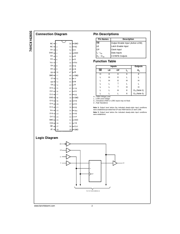
74VCX162835 Low Voltage 18-Bit Universal Bus Driver with 3.6V Tolerant Inputs/Outputs and 26Ω Series Resistors in Outputs
October 1998 Revised April 2000
74VCX162835 Low Voltage 18-Bit Universal Bus Driver with 3.6V Tolerant Inputs/Outputs and 26Ω Series Resistors in Outputs
General Description
The VCX162835 low voltage 18-bit universal bus driver combines D-type latches and D-type flip-flops to allow data flow in transparent, latched and clocked modes. Data flow is controlled by output-enable (OE), latch-enable (LE), and clock (CLK) inputs. The device operates in Transparent Mode when LE is held HIGH. The device operates in clocked mode when LE is LOW and CLK is toggled. Data transfers from the Inputs (In) to Outputs (On) on a Positive Edge Transition of the Clock.
 74VCX162835 Datasheet