Datasheet Details
| Part number | CY7C1473V25 |
|---|---|
| Manufacturer | Cypress (Infineon) |
| File Size | 428.71 KB |
| Description | (CY7C147xV25) 72-Mbit (2M x 36/4M x 18/1M x 72) Flow-Through SRAM |
| Datasheet |
 CY7C1473V25 Datasheet CY7C1473V25 Datasheet
|
|
|
Download the CY7C1473V25 datasheet PDF. This datasheet also covers the CY7C1471V25 variant, as both devices belong to the same (cy7c147xv25) 72-mbit (2m x 36/4m x 18/1m x 72) flow-through sram family and are provided as variant models within a single manufacturer datasheet.
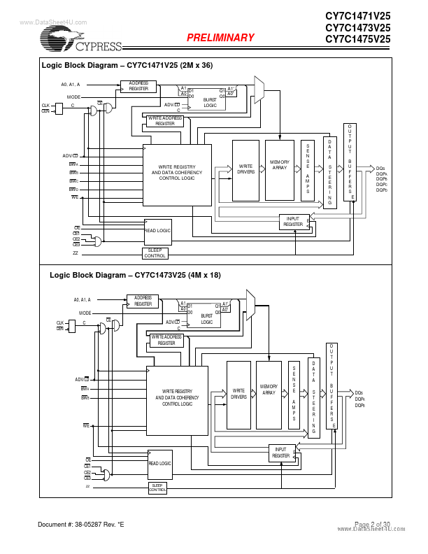
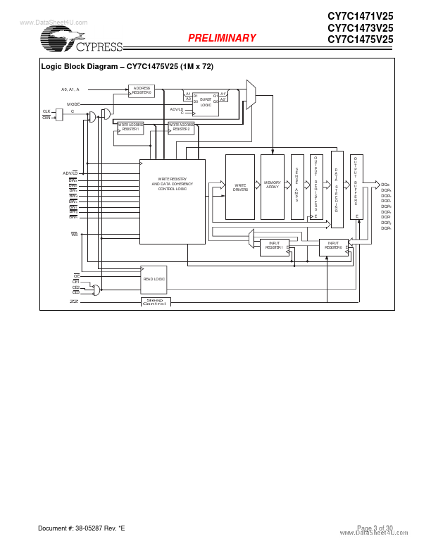
The CY7C1471V25, CY7C1473V25 and CY7C1475V25 are 2.5V, 2M x 36/4M x 18/1M x 72 Synchronous Flow-through Burst SRAMs designed specifically to support unlimited true back-to-back Read/Write operations without the insertion of wait states.
| Part number | CY7C1473V25 |
|---|---|
| Manufacturer | Cypress (Infineon) |
| File Size | 428.71 KB |
| Description | (CY7C147xV25) 72-Mbit (2M x 36/4M x 18/1M x 72) Flow-Through SRAM |
| Datasheet |
CY7C1473V25 Datasheet
|
|
|
|
| Part Number | Description | Manufacturer |
|---|---|---|
| CY7C1460SV25 | 36-Mbit (1M x 36/2M x 18) Pipelined SRAM | Cypress |
| CY7C1462SV25 | 36-Mbit (1M x 36/2M x 18) Pipelined SRAM | Cypress |
| CY7C1006D | 1-Mbit (256K x 4) Static RAM | Cypress |
| CY7C1011G | 2-Mbit (128K words x 16 bit) Static RAM | Cypress |
| CY7C1041G | 4-Mbit (256K words x 16 bit) Static RAM | Cypress |
| Part Number | Description |
|---|---|
| CY7C1473V33 | (CY7C147xV33) 72-Mbit (2M x 36/4M x 18/1M x 72) Flow-Through SRAM |
| CY7C1473BV33 | 72-Mbit (2 M x 36/4 M x 18) Flow-Through SRAM |
| CY7C147 | 4K x 1 STATIC RAM |
| CY7C1470BV25 | (CY7C147xBV25) 72-Mbit (2M x 36/4M x 18/1M x 72) Pipelined SRAM |
| CY7C1470BV33 | 72-Mbit (2 M x 36/4 M x 18/1 M x 72) Pipelined SRAM |