Datasheet4U Logo Datasheet4U.com

CY7C1021 - 64K x 16 Static RAM

Download the CY7C1021 datasheet PDF. This datasheet also covers the CY7 variant, as both devices belong to the same 64k x 16 static ram family and are provided as variant models within a single manufacturer datasheet.

Description

of read and write modes.

The input/output pins (I/O1 through I/O16) are placed in a high-impedance state when the device is deselected (CE HIGH), the outputs are disabled (OE HIGH), the BHE and BLE are disabled (BHE, BLE HIGH), or during a write operation (CE LOW, and WE LOW).

Features

  • High speed.
  • tAA = 12 ns.
  • CMOS for optimum speed/power.
  • Low active power.
  • 1320 mW (max. ).
  • Automatic power-down when deselected.
  • Independent Control of Upper and Lower bits.
  • Available in 44-pin TSOP II and 400-mil SOJ (BLE) is LOW, then data from I/O pins (I/O1 through I/O8), is written into the location specified on the address pins (A0 through A15). If Byte High Enable (BHE) is LOW, then data from I/O pins (I/O9 through I/O.

📥 Download Datasheet

Note: The manufacturer provides a single datasheet file (CY7-C1021.pdf) that lists specifications for multiple related part numbers.

Full PDF Text Transcription

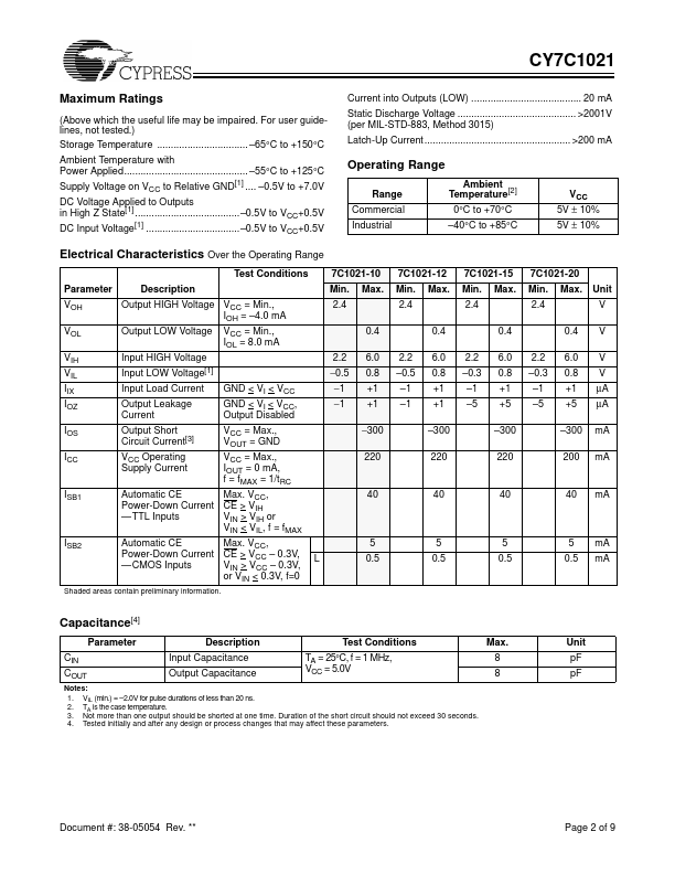
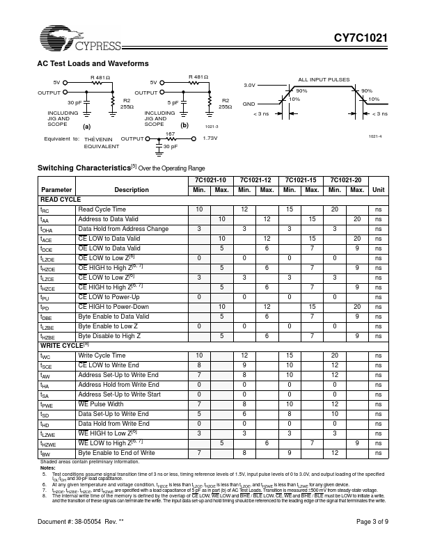
Click to expand full text
021 CY7C1021 64K x 16 Static RAM Features 
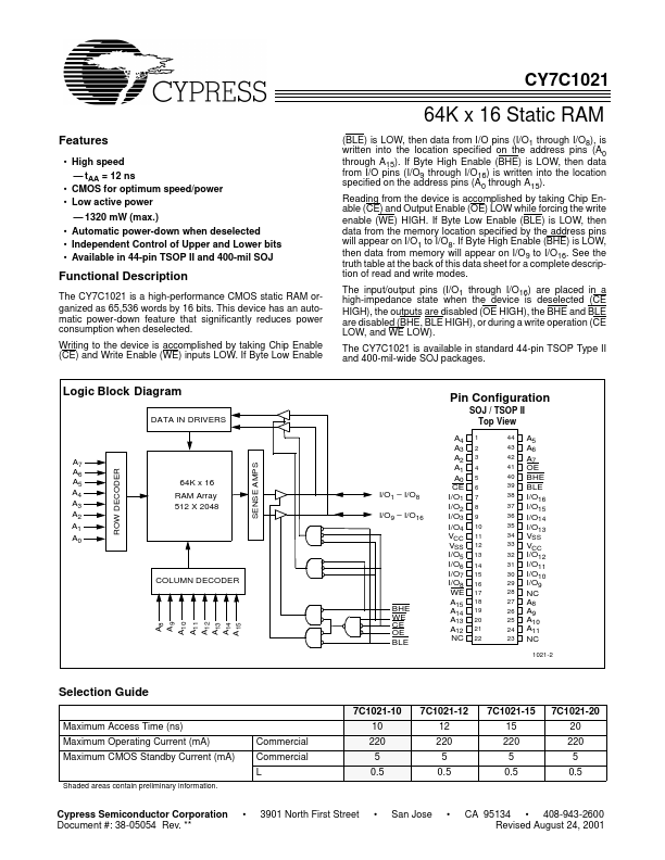
• High speed — tAA = 12 ns • CMOS for optimum speed/power • Low active power — 1320 mW (max.) • Automatic power-down when deselected • Independent Control of Upper and Lower bits • Available in 44-pin TSOP II and 400-mil SOJ (BLE) is LOW, then data from I/O pins (I/O1 through I/O8), is written into the location specified on the address pins (A0 through A15). If Byte High Enable (BHE) is LOW, then data from I/O pins (I/O9 through I/O16) is written into the location specified on the address pins (A0 through A15). Reading from the device is accomplished by taking Chip Enable (CE) and Output Enable (OE) LOW while forcing the write enable (WE) HIGH.
Published: |