Click to expand full text
1CY 7B9 92 0
fax id: 3516
CY7B9910 CY7B9920
Low Skew Clock Buffer
Features
• • • • • • • • • All outputs skew <100 ps typical (250 max.) 15- to 80-MHz output operation Zero input to output delay 50% duty-cycle outputs Outputs drive 50Ω terminated lines Low operating current 24-pin SOIC package Jitter: <200 ps peak to peak, <25 ps RMS Compatible with Pentium™-based processors
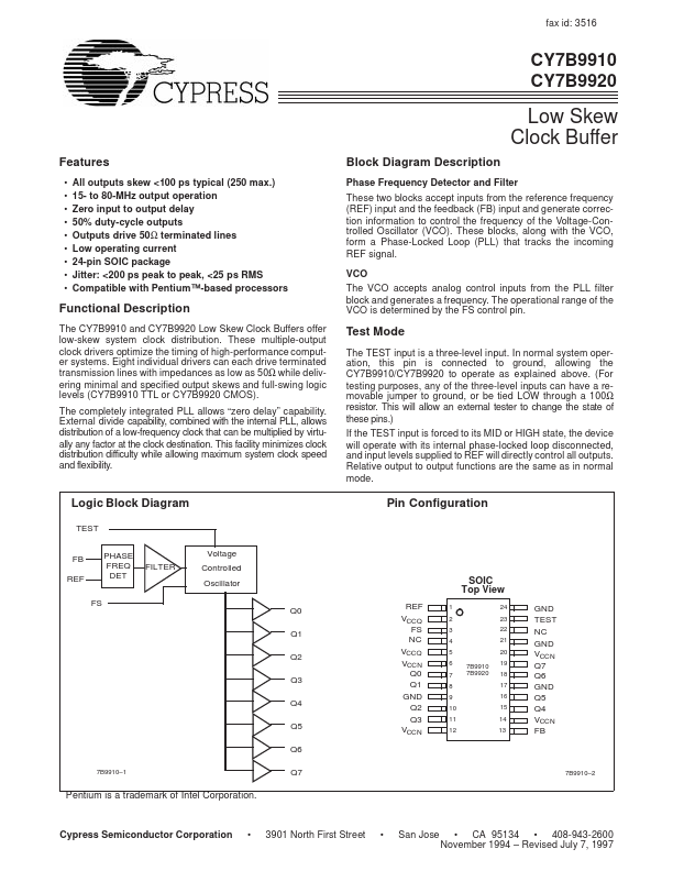
Block Diagram Description
Phase Frequency Detector and Filter These two blocks accept inputs from the reference frequency (REF) input and the feedback (FB) input and generate correction information to control the frequency of the Voltage-Controlled Oscillator (VCO). These blocks, along with the VCO, form a Phase-Locked Loop (PLL) that tracks the incoming REF signal.
 CY7B9920 Datasheet