Click to expand full text
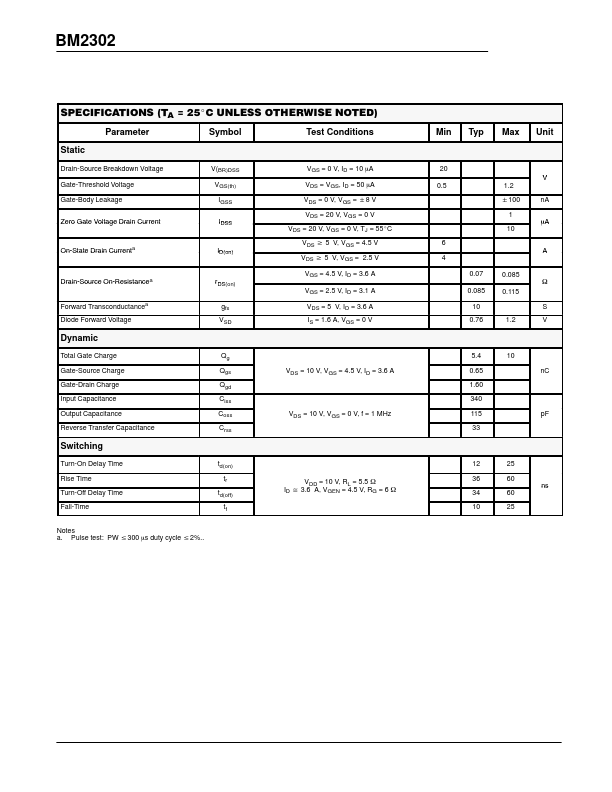
N-Channel 1.25-W, 2.5-V MOSFET
PRODUCT SUMMARY
VDS (V)
rDS(on) (W)
0.085 @ VGS = 4.5 V 20
0.115 @ VGS = 2.5 V
ID (A)
2.8 2.4
TO-236 (SOT-23)
G1 S2
3D
Top View
BM2302
ABSOLUTE MAXIMUM RATINGS (TA = 25_C UNLESS OTHERWISE NOTED)
Parameter
Symbol
Limit
Drain-Source Voltage Gate-Source Voltage Continuous Drain Current (TJ = 150_C)b Pulsed Drain Currenta Continuous Source Current (Diode Conduction)b Power Dissipationb
Operating Junction and Storage Temperature Range
TA= 25_C TA= 70_C
TA= 25_C TA= 70_C
VDS VGS ID IDM
IS PD TJ, Tstg
20 "12 2.8 2.2 10 1.6 1.25 0.80 –55 to 150
THERMAL RESISTANCE RATINGS
Parameter
Maximum Junction-to-Ambientb
Maximum Junction-to-Ambientc
Notes a. Pulse width limited by maximum junction temperature. b. Surface Mounted on FR4 Board, t v 5 sec. c.
 BM2302 Datasheet