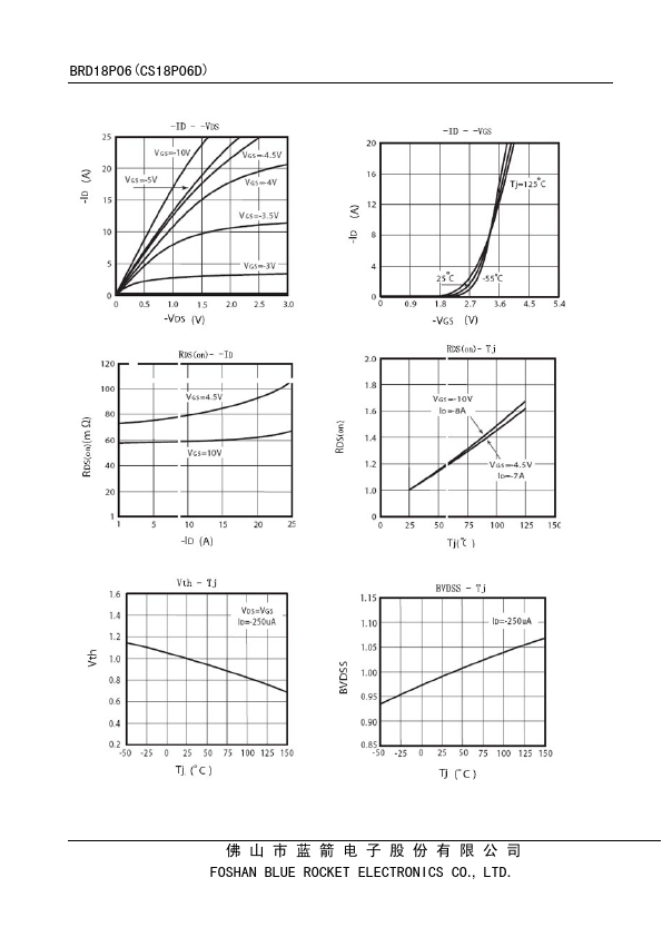
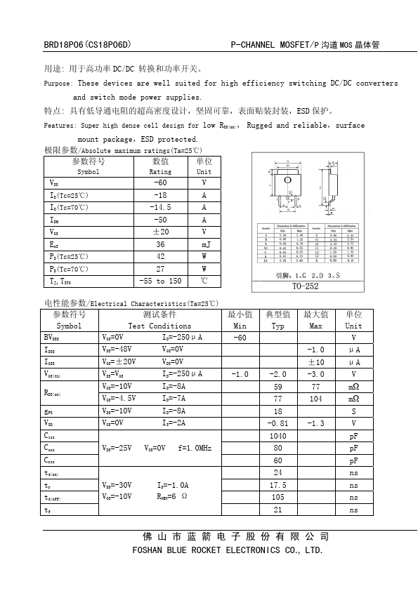
Super high dense cell design for low R ,DS(on) Rugged and reliable,surface
mount package,ESD protected. /Absolute maximum ratings(Ta=25℃)
Symbol
Rating
Unit
VDS ID(Tc=25℃) ID(Tc=70℃) IDM VGS EAS PD(Tc=25℃) PD(Tc=70℃) TJ,TSTG
-60 -18 -14.5 -50 ±20 36 42 27 -55 to 150
V A A A V mJ W W ℃
/Electrical Characteristics(Ta=25℃)
Symbol
Test Conditions
BVDSS
VGS=0V
ID=-250μA
IDSS
VDS=-48V
VGS=0V
IGSS
VGS=±20V
VDS=0V
VGS(th)
VDS=VGS
ID=-250μA
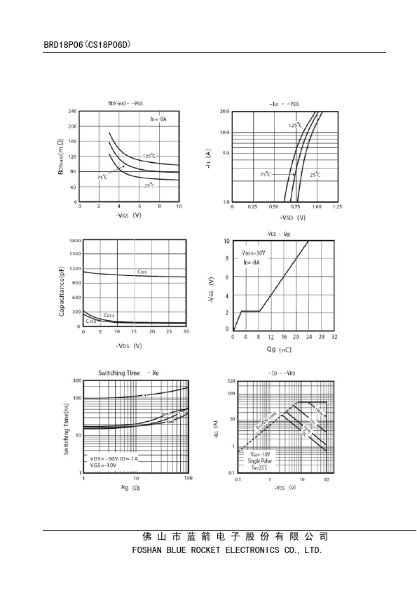
RDS(on)
VGS=-10V VGS=-4.5V
ID=.
Full PDF Text Transcription for CS18P06D (Reference)
Note: Below is a high-fidelity text extraction (approx. 800 characters) for
CS18P06D. For precise diagrams, and layout, please refer to the original PDF.
BRD18P06(CS18P06D) P-CHANNEL MOSFET/P MOS : DC/DC 。 Purpose: These devices are well suited for high efficiency switching DC/DC converters and switch mode power supplies. ...
View more extracted text
efficiency switching DC/DC converters and switch mode power supplies. : ,,,ESD 。 Features: Super high dense cell design for low R ,DS(on) Rugged and reliable,surface mount package,ESD protected. /Absolute maximum ratings(Ta=25℃) Symbol Rating Unit VDS ID(Tc=25℃) ID(Tc=70℃) IDM VGS EAS PD(Tc=25℃) PD(Tc=70℃) TJ,TSTG -60 -18 -14.5 -50 ±20 36 42 27 -55 to 150 V A A A V mJ W W ℃ /Electrical Characteristics(Ta=25℃) Symbol Test Conditions BVDSS VGS=0V ID=-250μA IDSS VDS=-48V VGS=0V IGSS VGS=±20V VDS=0V VGS(th) VDS=VGS ID=-250μA RDS(on) VGS=-10V VGS=-4.
 CS18P06D Datasheet