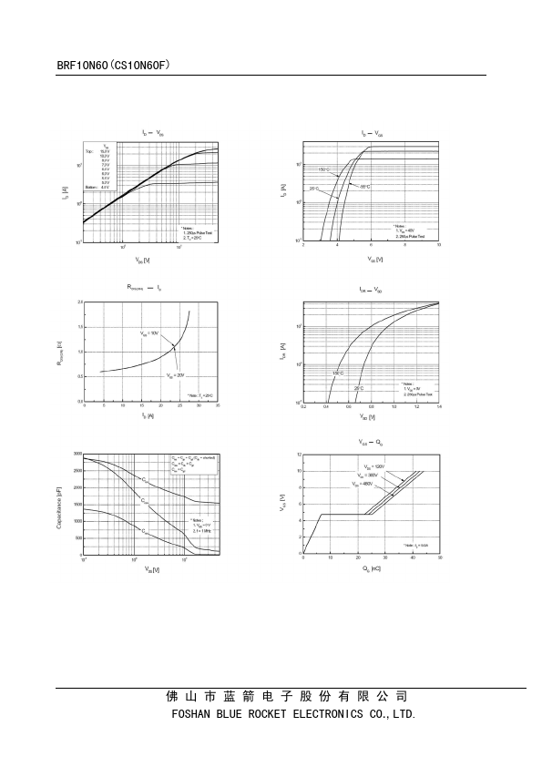
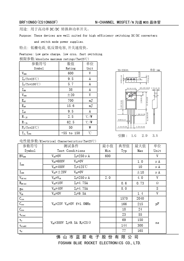
Low gate charge, low crss, fast switching. /Absolute maximum ratings(Ta=25℃)
Symbol
Rating
Unit
VDSS 600 V
ID(Tc=25℃)
9.5 A
ID(Tc=100℃)
5.7 A
IDM 38 A
VGSS
±20
V
EAS 700 mJ
EAR
15.6
mJ
IAR 9.5 A
RθJC 2.5 ℃/W
RθJA
62.5
℃/W
PD(Tc=25℃)
50 W
TJ,TSTG
-55 to 150 ℃
/Electrical Characteristics(Ta=25℃)
Symbol
Test Conditions
Min Typ Max
BVDSS
VGS=0V
ID=250μA
600
IDSS
VDS=600V VDS=480V
VGS=0V TC=125℃
IGSS VGS=±20V VDS=0V
1.0 10 ±10
VGS(th)
VDS=VGS
I.
Full PDF Text Transcription for CS10N60F (Reference)
Note: Below is a high-fidelity text extraction (approx. 800 characters) for
CS10N60F. For precise diagrams, and layout, please refer to the original PDF.
BRF10N60(CS10N60F) N-CHANNEL MOSFET/N MOS : DC/DC 。 Purpose: These devices are well suited for high efficiency switching DC/DC converters and switch mode power supplies. ...
View more extracted text
efficiency switching DC/DC converters and switch mode power supplies. : ,,。 Features: Low gate charge, low crss, fast switching. /Absolute maximum ratings(Ta=25℃) Symbol Rating Unit VDSS 600 V ID(Tc=25℃) 9.5 A ID(Tc=100℃) 5.7 A IDM 38 A VGSS ±20 V EAS 700 mJ EAR 15.6 mJ IAR 9.5 A RθJC 2.5 ℃/W RθJA 62.5 ℃/W PD(Tc=25℃) 50 W TJ,TSTG -55 to 150 ℃ /Electrical Characteristics(Ta=25℃) Symbol Test Conditions Min Typ Max BVDSS VGS=0V ID=250μA 600 IDSS VDS=600V VDS=480V VGS=0V TC=125℃ IGSS VGS=±20V VDS=0V 1.0 10 ±10 VGS(th) VDS=VGS ID=250μA 2.0 4.
 CS10N60F Datasheet