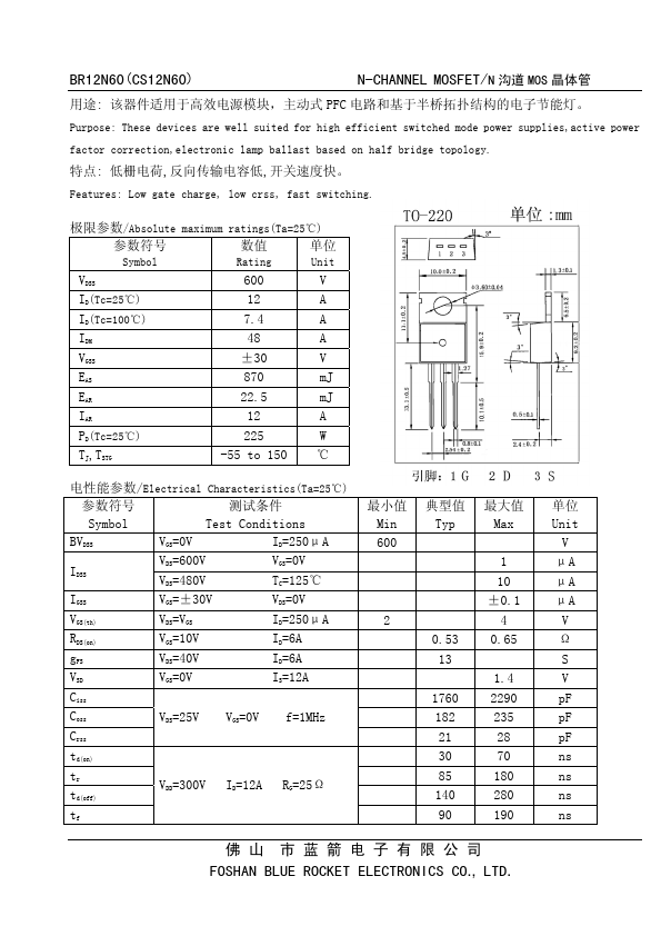
Low gate charge, low crss, fast switching. /Absolute maximum ratings(Ta=25℃)
Symbol
Rating
Unit
VDSS 600 V
ID(Tc=25℃)
12 A
ID(Tc=100℃)
7.4 A
IDM 48 A
VGSS
±30
V
EAS 870 mJ
EAR
22.5
mJ
IAR 12 A
PD(Tc=25℃)
225 W
TJ,TSTG
-55 to 150 ℃
/Electrical Characteristics(Ta=25℃)
Symbol
Test Conditions
BVDSS
VGS=0V
ID=250μA
IDSS
VDS=600V VDS=480V
VGS=0V TC=125℃
IGSS
VGS=±30V
VDS=0V
VGS(th)
VDS=VGS
ID=250μA
RDS(on)
VGS=10V
ID=6A
gFS
VDS=40V
ID=6A
VSD VGS=0.
Full PDF Text Transcription for CS12N60 (Reference)
Note: Below is a high-fidelity text extraction (approx. 800 characters) for
CS12N60. For precise diagrams, and layout, please refer to the original PDF.
BR12N60(CS12N60) N-CHANNEL MOSFET/N MOS : , PFC 。 Purpose: These devices are well suited for high efficient switched mode power supplies,active power factor correction,el...
View more extracted text
ficient switched mode power supplies,active power factor correction,electronic lamp ballast based on half bridge topology. : ,,。 Features: Low gate charge, low crss, fast switching. /Absolute maximum ratings(Ta=25℃) Symbol Rating Unit VDSS 600 V ID(Tc=25℃) 12 A ID(Tc=100℃) 7.4 A IDM 48 A VGSS ±30 V EAS 870 mJ EAR 22.
 CS12N60 Datasheet