Datasheet Details
| Part number | BLD6G22LS-50 |
|---|---|
| Manufacturer | Ampleon |
| File Size | 0.98 MB |
| Description | W-CDMA 2110 MHz to 2170 MHz fully integrated Doherty transistor |
| Datasheet |
 BLD6G22LS-50 Datasheet BLD6G22LS-50 Datasheet
|
|
|
Download the BLD6G22LS-50 datasheet PDF (BLD6G22L-50 included). The manufacturer datasheet provides complete specifications, pinout details, electrical characteristics, and typical applications for w-cdma 2110 mhz to 2170 mhz fully integrated doherty transistor.
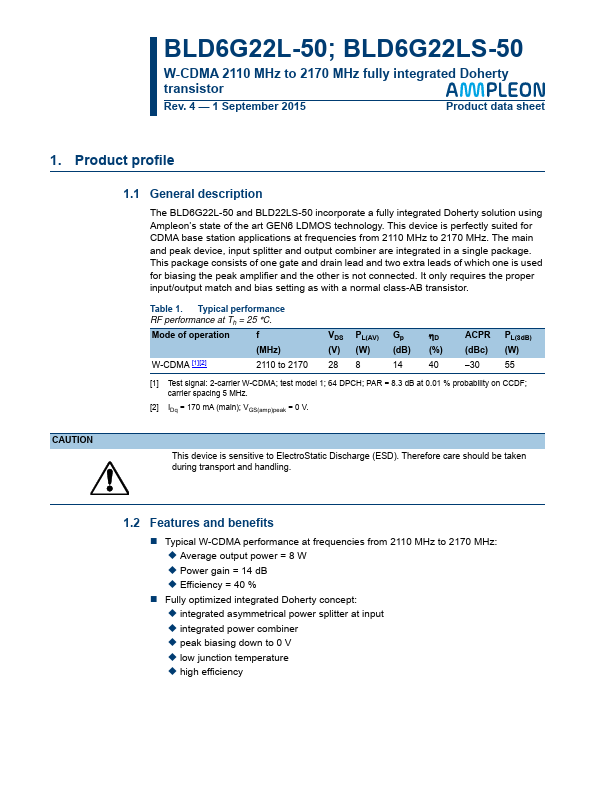
The BLD6G22L-50 and BLD22LS-50 incorporate a fully integrated Doherty solution using Ampleon’s state of the art GEN6 LDMOS technology.
This device is perfectly suited for CDMA base station applications at frequencies from 2110 MHz to 2170 MHz.
| Part number | BLD6G22LS-50 |
|---|---|
| Manufacturer | Ampleon |
| File Size | 0.98 MB |
| Description | W-CDMA 2110 MHz to 2170 MHz fully integrated Doherty transistor |
| Datasheet |
BLD6G22LS-50 Datasheet
|
|
|
|