AS7C1026
Features
- AS7C1026 (5V version)
- AS7C31026 (3.3V version)
- Industrial and mercial versions
- Organization: 65,536 words x 16 bits
- Center power and ground pins for low noise
- High speed
- 12/15/20 ns address access time
- 6, 7,8 ns output enable access time
- Low power consumption: ACTIVE
- 880 m W (AS7C1026) / max @ 12 ns
- 396 m W (AS7C31026) / max @ 12 ns
- Low power consumption: STANDBY
- 28 m W (AS7C1026) / max CMOS I/O
- 18 m W (AS7C31026) / max CMOS I/O
- Easy memory expansion with CE, OE inputs
- TTL-patible, three-state I/O
- JEDEC standard packaging
- 44-pin 400 mil SOJ
- 44-pin TSOP 2
- 48-ball 6 × 8 mm BGA
- ESD protection ≥ 2000 volts
- Latch-up current ≥ 200 m A
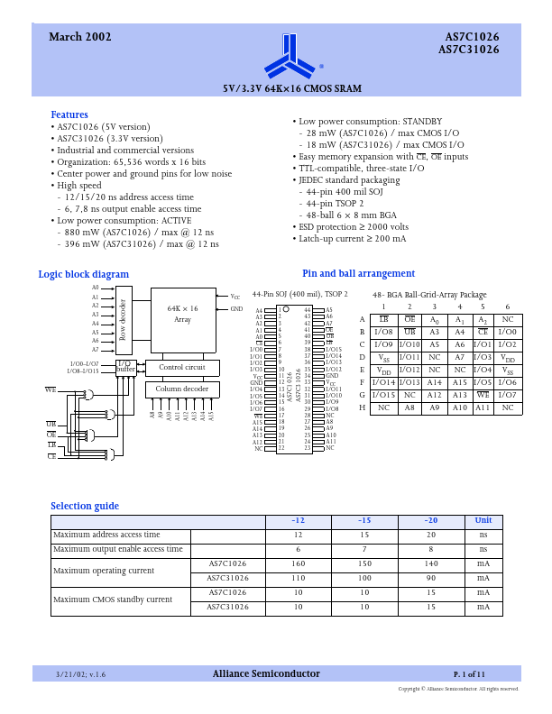
Logic block diagram
Row decoder
A0 A1 A2 A3 A4 A5 A6 A7
I/O0- I/O7 I/O8- I/O15
I/O buffer
UB OE LB
A8 A9 A10 A11 A12 A13 A14 A15
64K × 16 Array
Control circuit Column decoder
Pin and ball...