Click to expand full text
Data Sheet March 2000
ORCA® OR3LP26B Field-Programmable System Chip (FPSC) Embedded Master/Target PCI Interface
Introduction
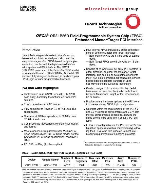
Lucent Technologies Microelectronics Group has developed a solution for designers who need the many advantages of an FPGA-based design implementation, coupled with the high bandwidth of an industry-standard PCI interface. The ORCA OR3LP26B (a member of the Series 3+ FPSC family) provides a full-featured 33/50/66 MHz, 32-/64-bit PCI interface, fully designed and tested, in hardware, plus FPGA logic for user-programmable functions.
s
Four internal FIFOs individually buffer both directions of both the Master and Target interfaces: — Both Master FIFOs are 64 bits wide by 32 bits deep. — Both Target FIFOs are 64 bits wide by 16 bits deep.
 OR3LP26B Datasheet