Datasheet Details
| Part number | CDCLVD2106 |
|---|---|
| Manufacturer | Texas Instruments |
| File Size | 837.62 KB |
| Description | Dual 1:6 Low Additive Jitter LVDS Buffer |
| Datasheet |
 CDCLVD2106 Datasheet CDCLVD2106 Datasheet
|
|
|
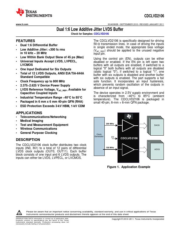
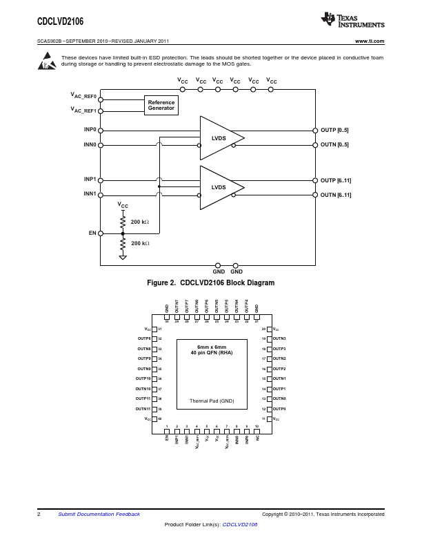
The CDCLVD2106 clock buffer distributes two clock inputs (IN0, IN1) to a total of 12 pairs of differential LVDS clock outputs (OUT0, OUT11).
Each buffer block consists of one input and 6 LVDS outputs.
The inputs can either be LVDS, LVPECL, or LVCMOS.
| Part number | CDCLVD2106 |
|---|---|
| Manufacturer | Texas Instruments |
| File Size | 837.62 KB |
| Description | Dual 1:6 Low Additive Jitter LVDS Buffer |
| Datasheet |
CDCLVD2106 Datasheet
|
|
|
|
| Part Number | Description | Manufacturer |
|---|---|---|
| CDCLD080 | SURFACE MOUNT SILICON CURRENT LIMITING DIODES | Central Semiconductor |
| CDCLD100 | SURFACE MOUNT SILICON CURRENT LIMITING DIODES | Central Semiconductor |
| CDCLD120 | SURFACE MOUNT SILICON CURRENT LIMITING DIODES | Central Semiconductor |
| CDCLD200 | SURFACE MOUNT SILICON CURRENT LIMITING DIODES | Central Semiconductor |
| CDCLD400 | SURFACE MOUNT SILICON CURRENT LIMITING DIODES | Central Semiconductor |
| Part Number | Description |
|---|---|
| CDCLVD2102 | Dual 1:2 Low Additive Jitter LVDS Buffer |
| CDCLVD2104 | Dual 1:4 Low Additive Jitter LVDS Buffer |
| CDCLVD2108 | Dual 1:8 Low Additive Jitter LVDS Buffer |
| CDCLVD110 | PROGRAMMABLE LOW-VOLTAGE 1:10 LVDS CLOCK DRIVER |
| CDCLVD110A | PROGRAMMABLE LOW-VOLTAGE 1:10 LVDS CLOCK DRIVER |
The following content is an automatically extracted verbatim text from the original manufacturer datasheet and is provided for reference purposes only.