Description
TB62713N/F
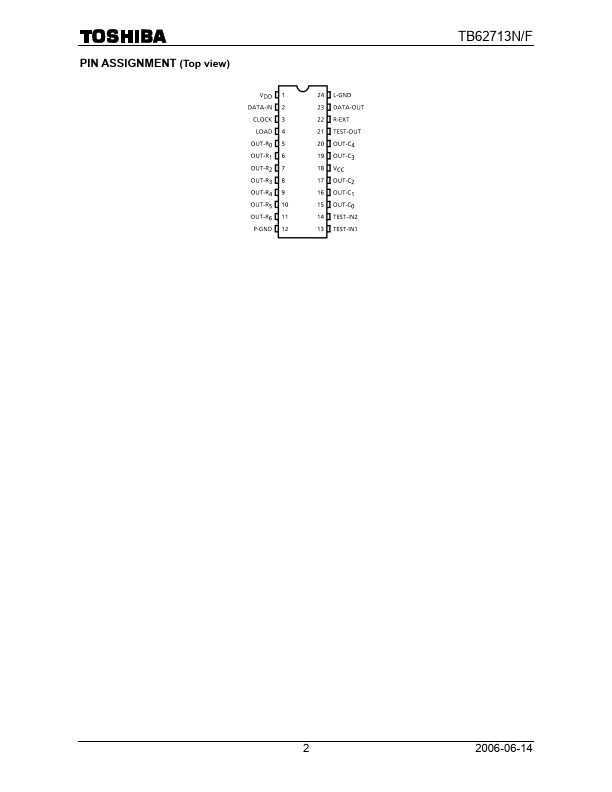
PIN NUMBER 1 2 3
4
5~11 12 13 14
15, 16, 17, 19, 20 18 21 22
23 24
PIN NAME
FUNCTION
VDD DATA
IN (DI)
5 V power pin.Serial data input pin.CLOCK (CK) Clock input pin.The shift register shifts data on the clock’s rising edge.LOAD (LD)
Load signal input pin.The data in the D8 to D15 bits of the 16
bit shift register.
Features
- Control circuit power supply voltage : VDD = 4.5 to 5.5 V
Digit output rating :.
- 17 V /.
- 350 mA
Row output rating : 17 V / 50 mA
Built.
- in decoder : Decoding based on ASCII code. Weight SDIP24-P-300-1.78: 1.62 g (typ. ) SSOP24-P-300-1.00: 0.32 g (typ. )
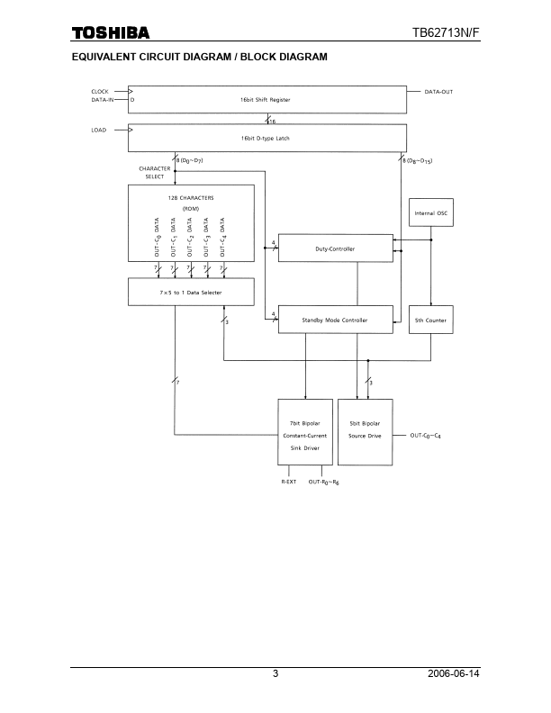
Digit control function : Automatically turns on column output OUT.
- C0 to OUT.
- C4 in sequence. Maximum transmission frequency (for serial data transmission) : fCLK = 15 MHz
Row output (OUT.
- R0 to OU.
 TB62713_Toshiba.pdf