Datasheet Details
| Part number | TB62713 |
|---|---|
| Manufacturer | Toshiba |
| File Size | 795.32 KB |
| Description | 7 x 5 DOT DISPLAY DECODER AND DRIVER |
| Datasheet |
 TB62713_Toshiba.pdf TB62713_Toshiba.pdf
|
| Part number | TB62713 |
|---|---|
| Manufacturer | Toshiba |
| File Size | 795.32 KB |
| Description | 7 x 5 DOT DISPLAY DECODER AND DRIVER |
| Datasheet |
TB62713_Toshiba.pdf
|
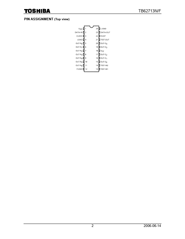
TB62713N/F PIN NUMBER 1 2 3 4 5~11 12 13 14 15, 16, 17, 19, 20 18 21 22 23 24 PIN NAME FUNCTION VDD DATA IN (DI) 5 V power pin.Serial data input pin.CLOCK (CK) Clock input pin.The shift register shifts data on the clock’s rising edge.LOAD (LD) Load signal input pin.The data in the D8 to D15 bits of the 16 bit shift register.
📁 TB62713 Similar Datasheet