Description
OF OPERATION
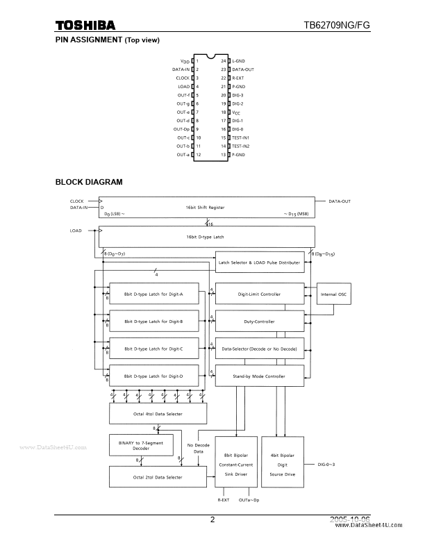
Data input (SERIAL
IN, CLOCK, LOAD) The data are input serially using the SERIAL
IN pin.
IN, LOAD, and CLOCK.
bit shift register offers control modes including duty Control Register Set, Digitset, Decode Set, and Standby Set, The data are shifted on the rising edge of the clock, starting from the MSB.
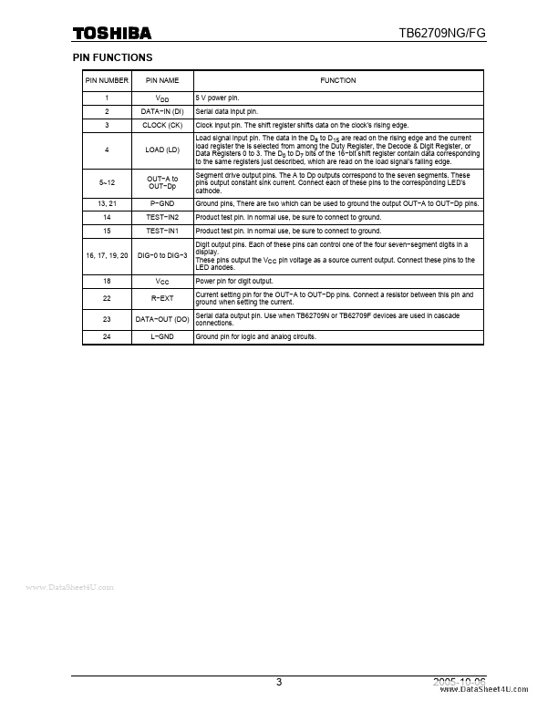
connecting TB62709NG or TB62709FG dev
Features
- Control circuit power supply voltage : VDD = 4.5 to 5.5 V Digit output rating : 17 V /.
- 400 mA Decoder output rating : 17 V / 50 mA Built.
- in decoder : Decodes the numerals 0 to 9, certain alphabetic characters, and of course blanks code. Digit control function : Can scan digit outputs DIG.
- 0 to DIG.
- 3 when connected to the common anode pins of a 7.
- segment display. Maximum transmission frequency : fCLK = 15 MHz Decoder outputs (OUT.
- A to OUT.
- Dp.
 TB62709FG_ToshibaSemiconductor.pdf