Description
Semiconductor Group
2
1998-10-01
HYB 39S16320TQ-6/-7/-8
www.DataSheet4U.com
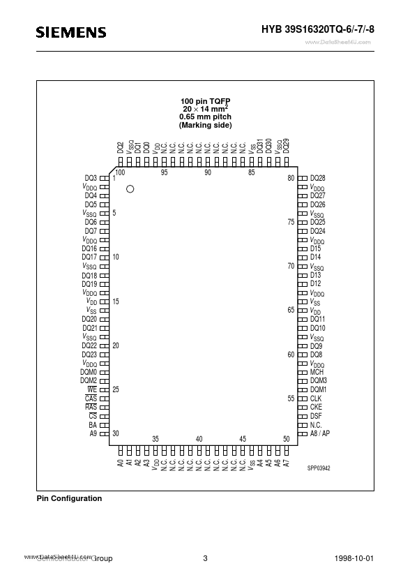
100 pin TQFP 20 × 14 mm2 0.65 mm pitch (Marking side)
DQ2 V SSQ DQ1 DQ0 V DD N.C.N.C.N.C.N.C.N.C.N.C.N.C.N.C.N.C.N.C.V SS DQ31 DQ30 V SSQ DQ29
DQ3 V DDQ DQ4 DQ5 V SSQ DQ6 DQ7 V DDQ DQ16 DQ17 V SSQ DQ18 DQ19 V DDQ V DD V SS DQ20 DQ21 V SSQ DQ22 DQ23 V DDQ DQM0 DQM2 WE CAS RAS CS BA A9
100 1
95
90
85
80
5 75
10 70
15 65
20 60
25 55
30
35
40
45
50
DQ28 V DDQ DQ27 DQ26 V SSQ DQ25 DQ24 V DDQ D1
Features
- These synchronous devices achieve high speed data transfer rates up to 143 MHz by employing a chip architecture that prefetches multiple bits and then synchronizes the output data to a system clock. The chip is fabricated with an advanced 64MBit DRAM process technology. The device is designed to comply with all JEDEC standards set for synchronous graphics DRAM products, both electrically and mechanically. RAS, CAS, WE, DSF and CS are pulsed signals which are examined at the positive edge of eac.
 HYB39S16320TQ-6_SiemensSemiconductor.pdf