Datasheet Details
| Part number | K4X1G163PC-LE |
|---|---|
| Manufacturer | Samsung Semiconductor |
| File Size | 564.86 KB |
| Description | Mobile DDR SDRAM |
| Datasheet |
 K4X1G163PC-LE Datasheet K4X1G163PC-LE Datasheet
|
|
|
Download the K4X1G163PC-LE datasheet PDF. This datasheet also covers the K4X1G163PC-L variant, as both devices belong to the same mobile ddr sdram family and are provided as variant models within a single manufacturer datasheet.
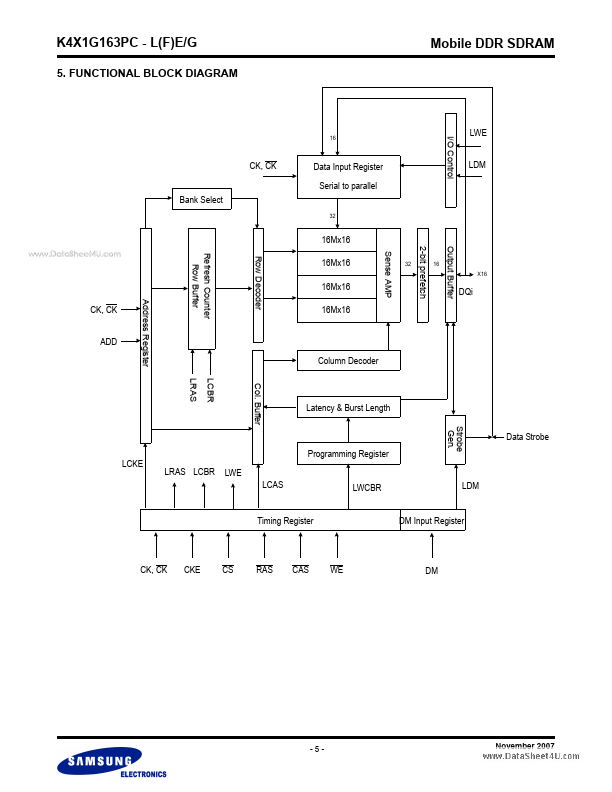
Clock : CK and CK are differential clock inputs.
All address and control input signals are sampled on the crossing of the positive edge of CK and negative edge of CK.
Internal clock signals are derived from CK/CK.
| Part number | K4X1G163PC-LE |
|---|---|
| Manufacturer | Samsung Semiconductor |
| File Size | 564.86 KB |
| Description | Mobile DDR SDRAM |
| Datasheet |
K4X1G163PC-LE Datasheet
|
|
|
|
| Part Number | Description | Manufacturer |
|---|---|---|
| K4X1G163PE-FGC6 | 64Mx16 Mobile DDR SDRAM | Samsung |
| K4X1G163PE-FGC8 | 64Mx16 Mobile DDR SDRAM | Samsung |
| K4X51163PG-FGC6 | 32Mx16 Mobile DDR SDRAM | Samsung Electronics |
| K4X51163PG-FGC7 | 32Mx16 Mobile DDR SDRAM | Samsung Electronics |
| K4X51163PG-FGC8 | 32Mx16 Mobile DDR SDRAM | Samsung Electronics |
| Part Number | Description |
|---|---|
| K4X1G163PC-LG | Mobile DDR SDRAM |
| K4X1G163PC-FE | Mobile DDR SDRAM |
| K4X1G163PC-FG | Mobile DDR SDRAM |
| K4X1G323PC-FE | 32Mx32 Mobile DDR SDRAM |
| K4X1G323PC-FG | 32Mx32 Mobile DDR SDRAM |
The following content is an automatically extracted verbatim text from the original manufacturer datasheet and is provided for reference purposes only.